Hello TI,
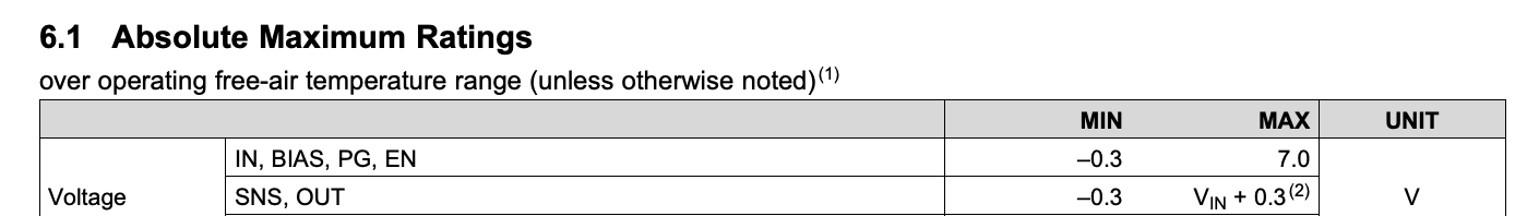
1> In case of LDO part TPS7A53 (3A or 4A part), to what voltage Power Good (PG) resistor should be pulled up to? What is recommended? Pull it up to Vin or Vout?
2> When we are driving EN signal of second TPS7A53 from PG signal of first TPS7A53 (for power sequencing) is it OK to have EN signal voltage more than Vin voltage? i.e. Vin = 3.3V and VEN = 5V or Vin = 1.8V and VEN = 3.3V?
Please let me know.
Thanks & Regards,
Prasad Gokhale