This thread has been locked.

If you have a related question, please click the "Ask a related question" button in the top right corner. The newly created question will be automatically linked to this question.

LM5166: 100mV Output Noise

Part Number: LM5166
Other Parts Discussed in Thread: ALLIGATOR, ,

My original thread was closed (https://e2e.ti.com/support/power-management/f/196/t/914047) so this is a follow up to that thread where we discussed different layout options. I was able to come back to this project and do some initial power up measurements.

This is a scope trace across the output cap using a wire for ground (so very short ground wire and probe position). I am feeding the board with 15VDC with my bench power supply and it is consuming 43mA. I've offset the channel by 5.0V so I could zoom in on the noise.

I literally just brought the board up but I've been curious how the output signal would look like since I was told that running the switcher trace under the input cap would not cause any noise issues. I'm not saying that my noise is from that but I'm certainly surprised to see 100mV on my first measurement.

  • George,

    Are you testing in PFM? Can you also scope the SW waveform?

    In PFM higher output ripple is expected, the converter does one or a few SW pulses to charge the output and then waits until the output discharges again.

    In PFM if your Ipeak greatly exceeds your average IOUT current then the output voltage will overcharge and output ripple can be expected.

    Does increasing the output current or capacitance reduce the output ripple?

    -Orlando

  • Hi Orlando,

    Here's my schematic and what the board is built with at this time:

    It's been a while since this board was designed so I need to dust off the cobwebs and remember what I was thinking! I remember now that in order to use the smaller inductor (22uH) I need to operate in PFM mode and with the 47Ω pull down on RT I'm operating in COT mode.

    I'll change R5 to a 0Ω so RT gets connected to ground and then do some additional measurements tomorrow and report back. I was just initially surprised at the high amount of ripple so I thought I'd get a post started so I could find out if this was related to layout at all.

    Thanks,

    George

  • I changed R5 to 0Ω so RT is now grounded and we should be operating in PFM mode. Here's a plot across Cout with 15V in and pulling 42mA:

    Here's the same plot but with the current draw down to 17mA:

    Here's the switching node (with 17mA draw) but using an alligator clip for the ground connection of the probe:

    Note that the current draw I mentioned above are the power supply values, not the load.

  • George,

    Your SW waveform does not look good, but the probe should be DC coupled for that.

    Looks like the pk-to-pk output ripple is the same for light load and medium load.

    This implies your peak current is consistent in PFM and the converter operation is stable.

    C1 is not necessary in this mode, but I don't think it is hurting.

    Is your output capacitor de-rating it's capacitance?

    When I quickly plug your design into the LM5166 quickstart tool ( LM5166DESIGN-CALC ), I'm seeing that a 47uF capacitor should result in 55mV of ripple.

    However ceramic capacitors lose effective capacitance when DC biased so I suspect that's related to what you see.

    Does increasing the output capacitor help?

    -Orlando

  • Hi Orlando,

    My output cap is a muRata GRM31CR61A476KE15, which is a 47uF, 10V, 1206 and looking at the DC Bias chart shows a 62% drop at 5V which is a little more than I was expecting. Here are some new scope shots retaken with the same setup as before for reference:

    And here are some plots with a 2nd 47uF output cap soldered on top of the original 47uF:

    So it looks like you were right and the output cap dropped it's capacitance too much. Let me know if you see anything else that I should take a closer look at or if this is the expected output waveforms under the light loads.

    -George

  • George,

    That SW waveform looks better!

    Ideally it should be closer to a square wave (and then ringing), right now the high-time looks like it slopes downward slightly (is your CIN far away from the IC?) but overall the SW node looks good.

    Otherwise everything looks pretty good.

    -Orlando

  • Hi Orlando,

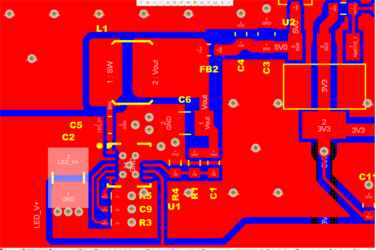
    The layout was reviewed in the other thread and although it went against my best practices the engineers in the thread said my layout was good. Here's a shot so you can see the placed of Cin (highlighted).

    I need to hook this up my programmable load and take some measurements under different loads but it is better than before.

    Thanks,

    George