This thread has been locked.

If you have a related question, please click the "Ask a related question" button in the top right corner. The newly created question will be automatically linked to this question.

LMZ23605: LMZ23605 output issue

Part Number: LMZ23605
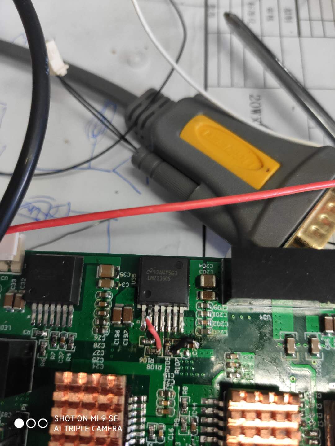
Other Parts Discussed in Thread: LMZM33606

I require a negative output from LMZ23605(-5.5V),but the chip give me a unstable -1.2V output(I can't use the -1.2V because it varies from -1.21 to -1.23 and never stop),my design is like this

help me with it,many thanks~~

  • why can't I watch the question in the forum?

  • The second pin shouldn't be connected to GND,should be conneted to output or just fload it.

  • Hi Wei,

    If synchronization is not needed, it should be connected to the system return path. In this case, it will be connected to the negative output since that is the system return path in IBB topology.

    Are you still having issues after this? It wasn't clear since you highlighted the thread as resolved and I just wanted to confirm that your issue is resolved or not. 

    Regards,

    Jimmy 

  • Hi,

         I  just floated the SYN pin and the issueh had been resolved. Thank you.

         I wonder why the chip works well while I didn't connet the SYN pin to the return path?Could I continue using it this way or SYN pin should be conneted to the output pin in case of shutting down?

  • Hi,

    I'd recommend connecting the SYNC pin to the return path if not used following recommendations in Section 7.3.1 for more information. In your system the return path is the negative output voltage or more specifically the AGND pin on the power module.

    Regards,

    Jimmy 

  • HI:

       I followed your advise and connected the SYN pin back to the negtive output pin,but the chip had broken down once, the Vout pin got shorted to the AGND pin.I can't figuer out the reason..

  • Hi,

    How many boards do you see this issue on? If you have another board, can you do the same test and have SYNC connected to negative output rail? In this case with the IBB conversion, the negative output rail will be on the bottom side of the bottom resistor (R109) and connected to pin4 of the power module.

    Regards,

    Jimmy

  • HI:

       Thanks for replying.I've got 2 boards.I did'nt connet the SYN pin to the 4th pin at the first time ,then the chip had broken down.So I conneted the SYN pin to R108(4th pin) by a short wire on my second board.But after a few day's using,the second chip had also broken down--just like the first one.Judging from your words, should I put R109 on the bottom side?I had put all the resistors and capacitors on the top side,the chip on the top side,too.

  • Hi,

    The bottom resistor is referring to Rfbb in the voltage divider network. It does not have to be on the bottom side of the PCB. 

    There is another error in your schematic, the soft-start capacitor(C70) should be connected to the return path (negative output voltage rail).

    I would suggest taking a new LMZ23605 unit and running stability and operational tests.

    Please make sure that all appropriate components are connected to system return path. The conversion from buck to IBB buck changed the return path into the negative output voltage rail. Components that used to connect to GND should now be connected to the negative output voltage rail. 

    Please retest your board with a new LMZ23605 device with the appropriate connections. 

    Regards,

    Jimmy 

  • I got it.I'll try it immediateliy.I didn't understand the return path in the right way.

  • Let me know if you have any other questions with this device.

    If you need some reading material to learn about the IBB conversion, please refer to this app note

  • Hi:

     Thanks a lot。I hadn't got any problem about this chip  these days!Thank you for solving my problem~

  • Thank you for using the E2E forum. If you have any remaining questions on this, please let me know.

    I will be closing this thread now.

  • emmm.The chip had continued breaking down...Even if I had connected SYN and C70 back to the negative output..I couldn't figure out why.

  • Hi Wei,

    What application are you using this IBB converted LMZ23605 in? Perhaps understanding this will help pinpoint the failure.

    Also  notice that the schematic doesn't have a clamp diode on the output. During startup, the output voltage rail will momentarily pull up because of the bypass capacitor between VIN and -VOUT. The clamp diode is to prevent the output voltage rail from going high and potentially causing issues in your application. 

    If you continue to have issues with the LMZ23605, perhaps you can try the LMZM33606 as an alternative. Here is an app note to provide some guidance on  the IBB conversion with actual test data using the EVM to detail how the device works when converted to IBB. 

    Lastly can you provide an update schematic and PCB layout of your board? The failure can be a combination of factors that attribute to the failure you see.

    Regards,

    Jimmy 

  • Hi:

           Thankyou for replying 。I didn't change my schematic and pcb layout,I had just fly some wires to the needed point.Can I just remove the C198(capacitor between Vin and Vout)?And I would connect a SMBJ5.0 between Vout and GND to see if it works.

  • Hi,

    The capacitor C198 is the Cio capacitor that is required in this IBB topology. Refer to Figure 9 and Section 5.2 for more information on this. 

    Please add the clamp diode and retest again. 

    Regards,

    Jimmy 

  • I see.Thanks.

  • Please keep me updated on your test results with the Cio and clamp diode populated in your IBB application test.

    Regards,

    Jimmy

  • This thread will be closed due to inactivity.

    Thank you for using the forum.

    Regards,

    Jimmy