This thread has been locked.

If you have a related question, please click the "Ask a related question" button in the top right corner. The newly created question will be automatically linked to this question.

TPS55340: VIN and GND shorted after first power up and then applying power to EN

Part Number: TPS55340

Hello,

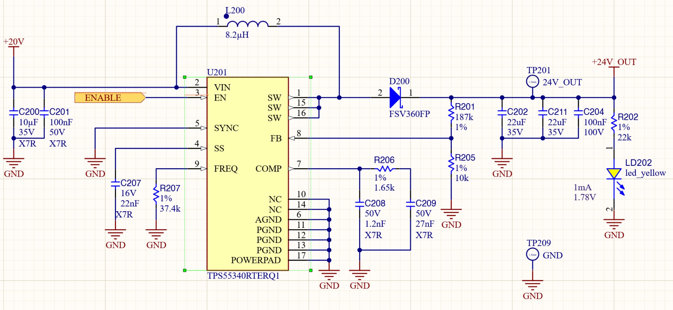
I am having the following issue with your TPS55340 device (designed for a 24V output @1A output)

  1. 20V (constant) applied to VIN (VBAT pin) and no load connected to output (apart from LED). 
  2. 20V applied to ENABLE pin ()
  3. Instantly +20V and GND become shorted (even with a very small current limit in place)
  4. Removing regulator from PCB removes short

I have performed the following checks:

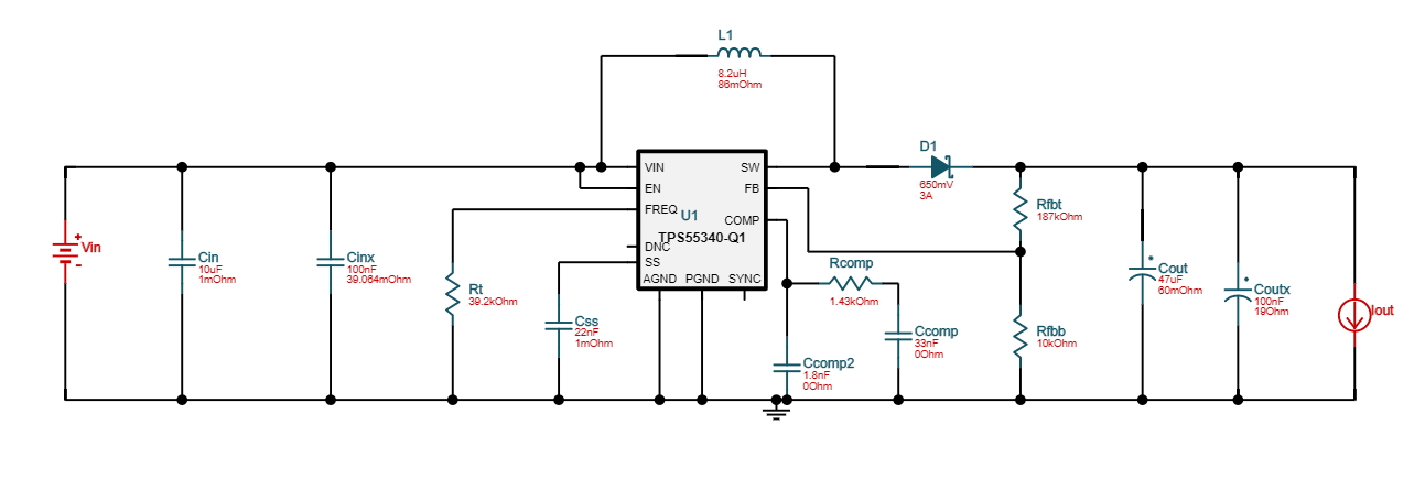
  • Circuit simulated on Webench
  • Fitted BOM confirmed with Webench
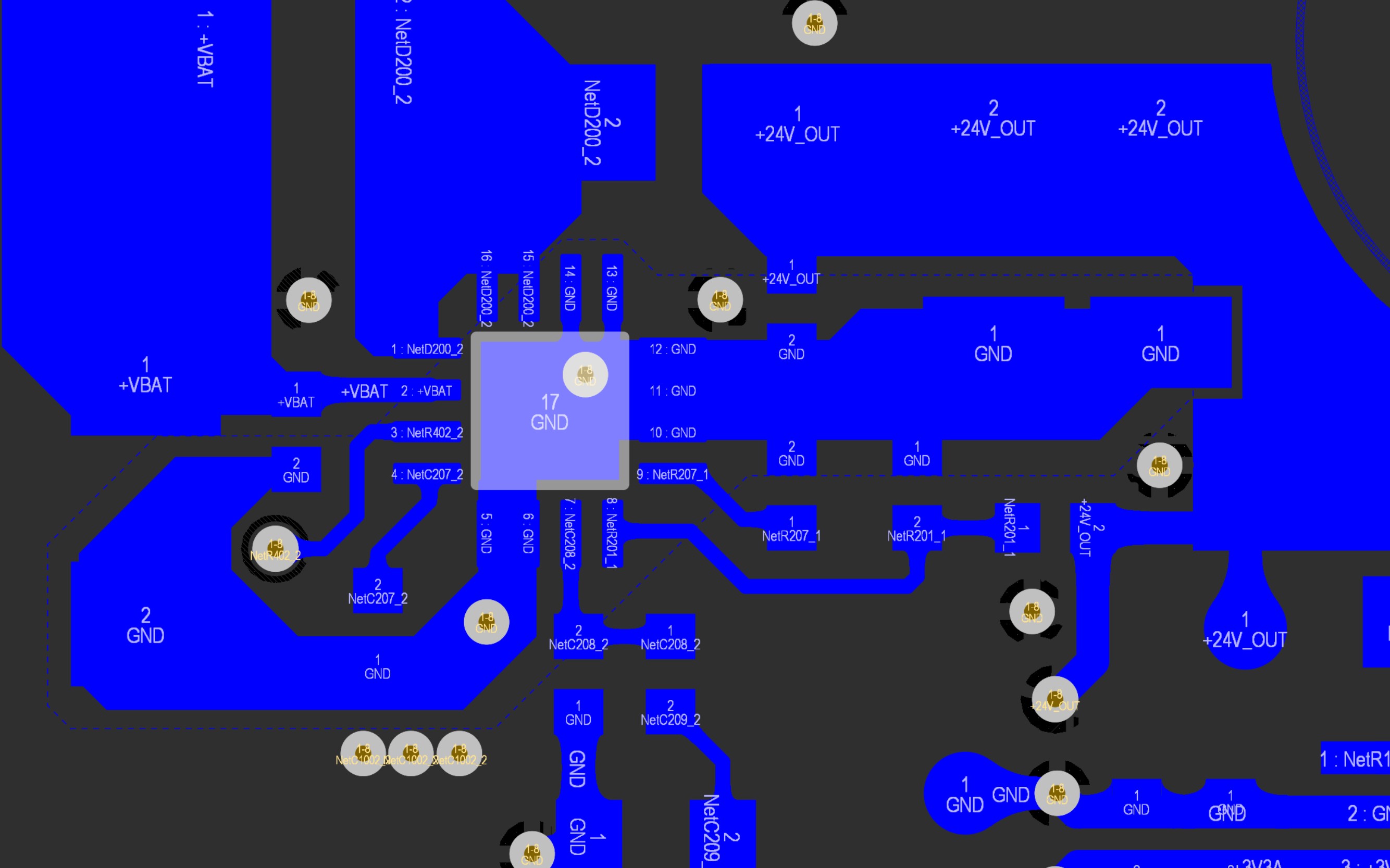
  • PCB checked for shorts/damage/soldering quality
  • Tried on a second PCBA

Do you have any idea what else could be checked? Thanks in advance.

  • Hello Josh,

    Is the layout a 2-layer board? If yes, please check the middle via of the 3 on the right side. The signal that is going to the via is the 24V output voltage, but it looks as if this via is shorted to GND on the bottom side.

  • Hello Brigitte,

    The board is actually 8 layers and so this should be OK.

    Thanks.

  • Hello Brigitte,

    I have just noticed the following, can you confirm that at the frequency our design is operating, there should be no issue with only a 2mA load.

    From the TPS55340-Q1 January 2019 datasheet:

    When using the internal switching frequency above 1.2 MHz, the TPS55340-Q1 device might not pulse skip as described in the Minimum On Time and Pulse Skipping section.

    From WEBENCH:

    For frequency > 1.6 MHz, the user is required to make sure load current is always greater than "Iout Min" value shown in the Op Vals.


    Thanks.

  • Hi Josh,

    It's possible that the output voltage overshoot at light load, which could damage your 35V capacitor and even the IC itself.  Could check the following on PCB, after disconnecting both the load and input source.

    1. if you see permanent short across SW to GND--placing multi meter positive lead at SW, and negative at GND)-then the IC is damaged.

    2. If you see permanent short across the output capacitors, then your output capacitor is damaged. 

    To avoid the situation mentioned in the datasheet, you should consider to reduce the switching frequency to 1.2MHz or lower.

    Thanks,

    Youhao Xi, Applications Engineering

  • Hi Youhao,

    Could you just confirm the following for me?

    • Currently the regulator cannot enter pulse skipping mode as the switching frequency is too high?
    • If I set the switching frequency to 1.185MHz, the regulator will be able to enter pulse skipping mode and I will not need to have a minimum load connected? Is this far enough below 1.2MHz to guarantee that the pulse skipping mode can be entered?
    • When the regulator is working in pulse skipping mode, there is no danger of a large spike damaging the regulator or output components?
    • Why does WEBENCH mention 'For frequency > 1.6 MHz, the user is required to make sure load current is always greater than "Iout Min" value shown in the Op Vals' and not 1.2MHz as in the datasheet?

    Please note, as mentioned above, I have removed the regulator from the PCB and this removes the short between supply and return.

    Many thanks,

    Josh

  • Hi Josh,

    Answers to your questions in the same order (pardon me for not copying over your original questions):

    • Yes, it is possible that the IC may not be able to enter the pulse skipping mode.
    • According to the datasheet, the IC should enter the pulse skipping mode.
    • In pulse skipping, it regulates the output voltage so no risk of over voltage to cause damage.  Only it cannot enter the pulse skipping the Vout can run away.
    • It might be a typo, which I need to notify our Webench group.  Anyway, Webench and design calculators are developed to help customers in the design, and mistakes may exist, and we will correct once noticed.  Please always follow the datasheet recommendations if you see a discrepancy in our supporting materials. 

    Thanks,

    Youhao

  • Hi Youhao,

    I have modified the design to give a switching frequency of 1.185MHz, which should in theory allow the pulse skipping mode to be entered (see below diagram). When I powered the regulator on the updated design from a 20V supply and then connected EN to 20V, a 24V output was established as expected. Unfortunately when I removed the EN connection to 20V and reapplied it, the 24V output didn't recover and the supply voltage and ground became shorted.

    FYI: The load connected to the 24V rail was 100mA generated by an electronic load which was permanently enabled. When the TPS55340QRTERQ1 device was removed from the PCB, the short between the supply rail and ground was removed, all other components appear to be in working order.

    Many thanks,
    Josh

  • Hi Josh,

    First, our Webench group experts are updating the model to reflect the warning about the 1.2MHz.

    I need to take a further study of your case, and get back to you  o later than COB Wednesday next week.

    Best Regards,

    Youhao

  • Many thanks Youhao.

  • Hi Josh,

    Sorry for the delay.  First, our Webench group has updated the model and the warning is now present underneath the schematic, regarding the switching frequency.  Again, thank you for your input which brought our attention to this matter.

    Regarding your updated schematic (a copy from Webench?), I cannot find any obvious problem and the circuit should work.  I am afraid the circuit may be damaged when you remove the EN, and when you reapply  it to VIN you just see the already damaged circuit. How do you remove the EN from VIN?  I don't see from the schematic that you circuit has electronic control.  Did you physically pulled off from VIN?  If you do so, ESD may damage the IC.

    Anyway, the layout picture does not reveal much.  To better understand the issue, could you capture the following waveforms on the same scope picture?

    • SW voltage
    • Vout
    • SS voltage
    • EN

    We would like to see how these signals respond to the EN signal (removal from VIN, and re-apply to the VIN), both events. 

    Please show an overview, the zoom in around any abnormal transients on the overview.

    Thanks,

    Youhao

  • Hi Youhao,

    I have tried the previously mentioned modification (switching frequency change) on another of our PCBAs, this time toggling the EN pin of the TPS55340 using a GPIO of a processor; this so far seems to be successful. The only difference here is that the EN is not being enabled using a separate 20V from our PSU. Is it possible to damage the device if the EN signal is larger than VIN and is the maximum voltage on EN really 38V? I am a little worried about using such a device in our design which is so easily damaged.

    Best regards,
    Josh

  • Hi Josh,

    Thank you for the update, and I am glad you get the circuit working now.

    Note that EN pin's abs max rating voltage is 34V, not 38V.  And we recommend 32V max for EN pin.  It should not damage the IC if EN is greater than VIN. 

    If your external signal to control EN is greater than the EN rating, you may insert a resistor divider to scale down the voltage applied to the EN pin.

    Again, please be careful when working on the IC, especially pay attention not to damage the IC by ESD. 

    Best Regards,

    Youhao