This thread has been locked.

If you have a related question, please click the "Ask a related question" button in the top right corner. The newly created question will be automatically linked to this question.

UCC21750-Q1: What kind of issue would caused by the copper under body

Part Number: UCC21750-Q1

Hi Team,

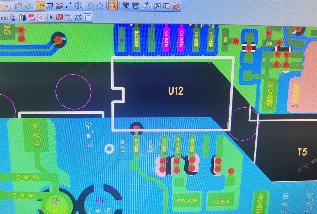
  My customer now is evaluating UCC21750-Q1,  and during the PCB layout, the copper is under the UCC21750-q1's body, PCB layout shown as below figure,

and in datasheet there is description that "No PCB trace or copper is allowed under the gate driver.A PCB cutout is recommended to avoid any noisecoupling between the input and output side which can contaminate the isolation barrier",  

  Could you kindly share more information how the PCB layout impact the isolation barrier?

Best Regards

Benjamin

  • HI Benjamin,

    Thanks for your question.

    One important reason that pours/traces are not allowed under the package is that it reduces the effective creepage/clearance of the barrier and thus the driver.

    Another reason, which is just as you said: that copper pours or traces should not be routed underneath the IC package of isolated driver are that interference (such as from output switching transient) can be coupled onto low-voltage power ground planes and signal traces or vice versa.

    Also: the driver package are also creepage and clearance, from package and leads for example, are critically related to the isolation ratings of the device. If traces or planes between HV and LV are routed under the IC it effectively reduces the function of the driver isolation.

    This concept is evident from narrowbody vs. widebody package. Even if the capacitive isolation inside the driver is rated at 5.7kVrms, if the leads of LV and HV side get closer and closer together, the conductors (leads) get closer and closer together, reducing the airgap, so the isolation of the driver can become a function of the package rather than the effectiveness of the isolation technology in the IC.

    This same concept goes for PCB traces, they are also conductors, seperated by a soldermask filled gap. The closer they get, the more the HV and LV side becomes coupled, and the less air/soldermask there to keep the HV side from arcing over and to minimize coupling.

    Routing power and signal under the driver could even result in arc/short from HV to LV side through the solder mask in situations where the driver would isolate this from the LV side or fail-open. it is always important to pay close attention to the PCB layout, because the gate driver is only part of the system.

    These concepts are equally applicable to transformer and optocoupler-based drivers as well. They are not exclusive to capacitive isolation.

    I hope this answers your question, let me know if you have any followup questions.

    Best

    Dimitri

  • Hi Dimitri,

      Very appreciated for your clarification. Customer has modified the PCB layout.

    Best Regards

    Benjamin