This thread has been locked.

If you have a related question, please click the "Ask a related question" button in the top right corner. The newly created question will be automatically linked to this question.

BQ40Z80: request for design review - BQ40Z80

Part Number: BQ40Z80

Hi,

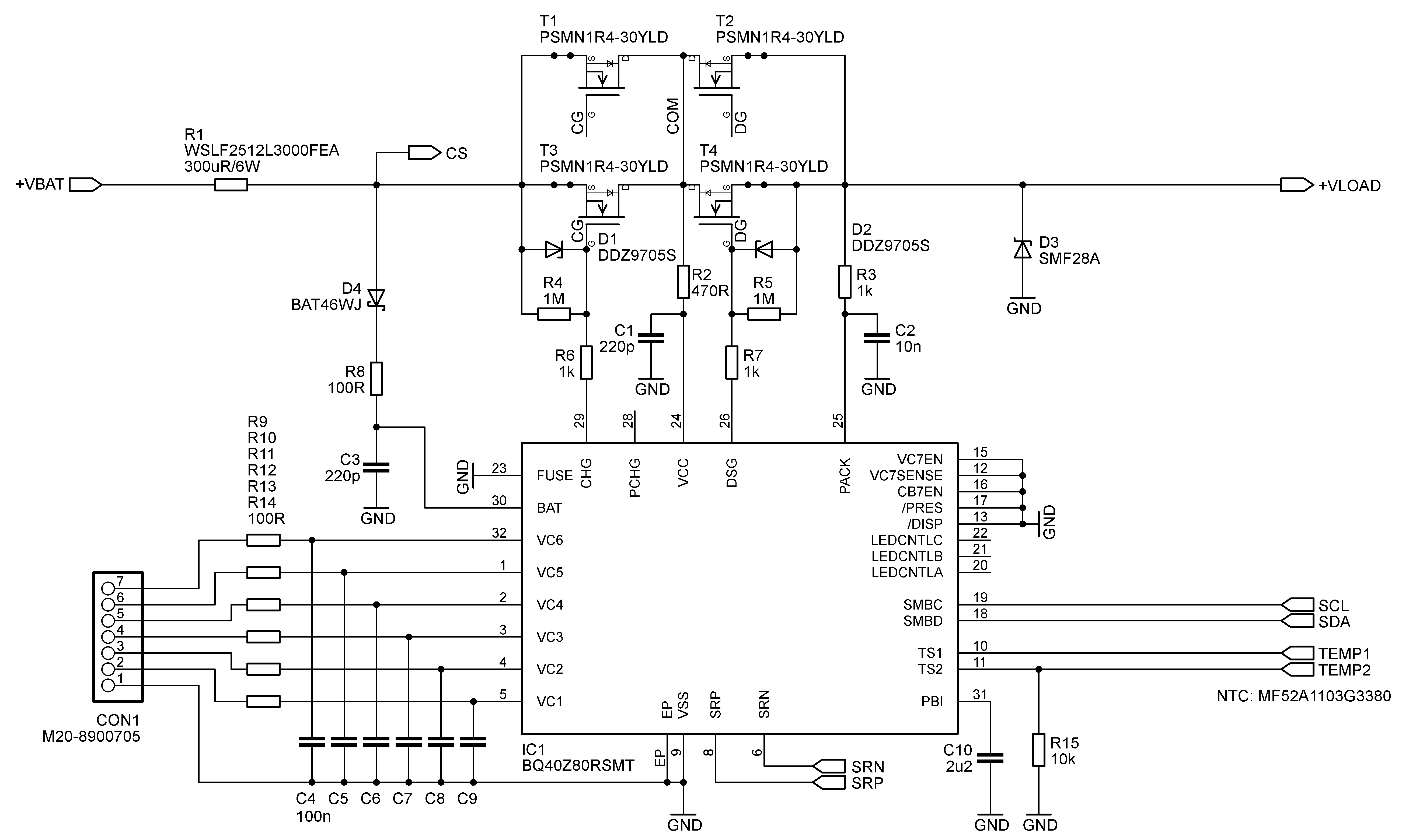
I kindly request a review of the attached design with respect to the correct BQ40Z80 wiring, and values of associated components. In particular, I am unsure about the values of these components:
- R8, C3, R6, R2, C1, R7, R3, C2.

I have a few other questions and remarks:
- the cell voltage sense connections including VSS (CON1) can make contact in any order, is this acceptable for the IC?
- the +VBAT power connection to the battery can be made before or after connecting CON1 during production, which order is preferable?
- the second temperature input (TS2) is active but not used, therefore a default 10k resistor (R15) is in place.
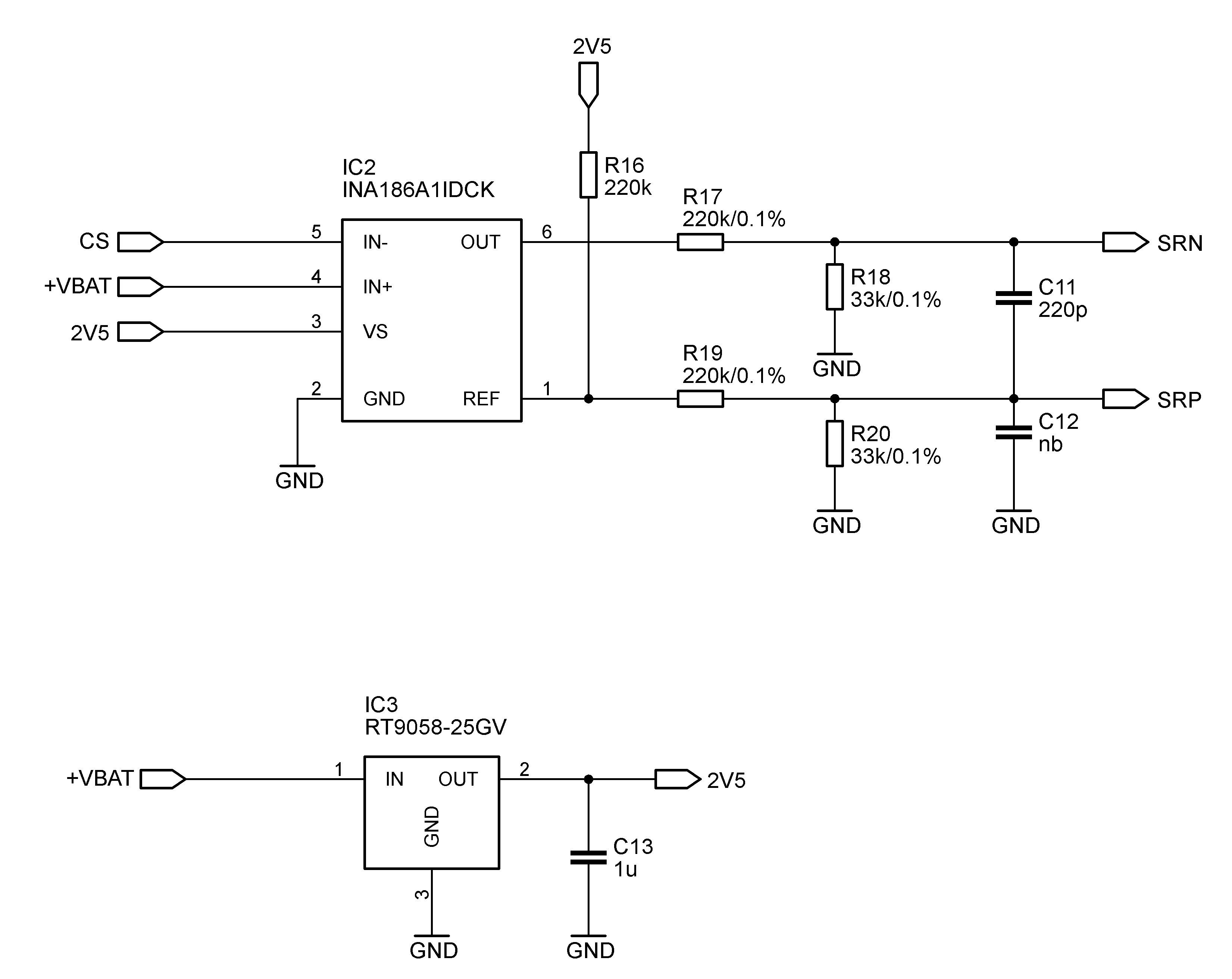
- the second page shows the high side current monitoring circuit for completeness, this part is fully evaluated and only provided for completeness.

Thank you in advance,
Regards
Frank Boeh

  • Hello Frank,

    One thing that I am concerned about is  that I see no GND to respect to +VLOAD. I am assuming that you have D3 for ESD protection. To properly connect this, you would have to have D3's GND to respect to +VLOAD(So it'd be -VLOAD), not your current GND(BAT-).

    Regarding the values for your components, they all should work fine with your design. 

    As for your questions, yes, you can connect the cells in any order you want. If you use secondary protection it could blow a FUSE, so it isn't recommended in that scenario. But looking at your schematic, you don't have anything to worry about.The order of connection shouldn't really matter(CON1 vs BAT+) if all is connected properly, however, I'd connect CON1 first just in case.

    Best Regards,

    Luis Hernandez Salomon

  • Luis H. S. said:
    One thing that I am concerned about is  that I see no GND to respect to +VLOAD. I am assuming that you have D3 for ESD protection. To properly connect this, you would have to have D3's GND to respect to +VLOAD(So it'd be -VLOAD), not your current GND(BAT-).

    My rationale here is protecting the chips from inductive kickback induced voltage spikes when the BMS disconnects a load or short circuit under high current. I expect this to be more prominent at the load side, as the cable loop is much longer there (~ 600mm) compared to the battery leads (~ 150mm). As the chips 'see' voltages with respect to GND, the protection should be effective even though the return path uses the most negative balancer lead. The (removable) connected load has its own protection. ESD is not my target here, as the BQ40Z80's should have built in protection and I'll check in the design if that is effective enough. Does that all sound reasonable?

    Luis H. S. said:
    The order of connection shouldn't really matter(CON1 vs BAT+)

    When connecting BAT+ first, and then inserting the balancer plug, it would be possible that e.g. VC2 gets connected first. In this case, I would expect that the BQ40Z80 would be powered parasitically via the input protection diodes. Should I consider this as problematic? I am asking to this detail, because we had been using a different chip before (ISLISL94202), which was failing destructively in the field. Neither I nor the Intersil engineers were able to track this down.

    Thanks for confirming the other topics!

    Regards

    Frank

  • Hello Frank,

    What voltage spikes are you expecting? You just have to be careful such that the voltage into the pins does not exceed to ABS Max as shown in the datasheet(Section 7.1) in such cases. Usually adjusting the series resistances into the pins according to the expected voltage spike is enough to protect against them. Although the BQ40Z80 does offer some protection, we always recommend to add some ESD protection to protect the protection FETs. 

    Something new I noticed, I see you shorted many unused pins to GND. I believe you can just leave these open if unused. However, for the PIN17(PRESS), if you are using it for System Present, you would need to use a resistor to pull-down the pin. See Section 9.2.2.3.3 of the datasheet for more information.

    Order of connection should not matter when connecting the device. The BQ40Z80 should have no issues. Usually if the battery is not connected, the device will be off unless there's a voltage across VLOAD. Even if the battery pack is connected, it will remain off unless you apply a voltage across VLOAD so that there's a voltage in the PACK pin and the device can go wake-up. After the device is waken up, you can remove the voltage across VLOAD and the device will stay on through the battery pack.

    Glad to help!

    Best Regards,

    Luis Hernandez Salomon

  • Hi Luis,

    thanks for responding so quickly, that is really helpful to push this redesign.

    "What voltage spikes are you expecting"
    >> we are seeing max. 10V excess ringing at +VLOAD with respect to BMS GND for a few microseconds from a short circuit disconnect without TVS diodes. Redesigned prototypes will be ready by mid next week, and I'll carefully check all high-side voltages that the chips 'see'.

    "series resistances into the pins according to the expected voltage spike is enough to protect against them"
    >> that's also my working basis, which is why I added R's and C's to each of them to be on the safe side.

    "ESD protection to protect the protection FETs"
    >> as the MOSFET D-S path acts as a fast and capable zener diode when in avalanche along with some capacitance, I usually have very good results without any extra protection (except at the gate). In another project (3-phase motor driver) we can shoot 4kV HBM directly into the switching node without any damage.

    "I see you shorted many unused pins to GND. I believe you can just leave these open if unused"
    >> I was following the datasheet recommendations from the individual pin descriptions on page 4, saying "if not used, tie to GND". I deviated from this for LEDCNTA/B/C, where the datasheet say pull down with 20k. I just don't have space for that which is why I had to omit them. I am worried about cross current from floating potentials at the input of traditional CMOS input structures, would that not be the case here?

    "for the PIN17(PRESS), if you are using it for System Present"
    >> that feature is disabled in the configuration (NR=1), the chip is used 'always on' but with significantly reduced sampling intervals to keep the quiescent current low enough.

    "Usually if the battery is not connected, the device will be off unless there's a voltage across VLOAD. Even if the battery pack is connected, it will remain off unless you apply a voltage across VLOAD so that there's a voltage in the PACK pin and the device can go wake-up. After the device is waken up, you can remove the voltage across VLOAD and the device will stay on through the battery pack."
    >> perfect, that matches our current production flow.

    Regards Frank

  • Hello Frank,

    Perfect, if you've already  accounted the voltage spikes into your values, you should have no issues.

    You can leave the LEDCNT pins floating if you cannot place the 20k-Ohm resistors to GND. As for the other pins, if the datasheet recommends to short to ground, then it's best to leave them as it is currently and configure it as such. You can see pin diagram equivalents in the datasheet if you want to have a better idea on how some of these pins behave.

    Let us know if you have any further questions.

    Best Regards,

    Luis Hernandez Salomon

  • Hi Luis,

    thanks for confirming, should be all set then!

    Regards

    Frank

  • Hi Luis,

    I need to reopen this thread, as the solution does not work as intended. Details in next post.

    Regards

    Frank

  • Please post a different thread so we can close this original. You can reference back to this particular thread.