This thread has been locked.

If you have a related question, please click the "Ask a related question" button in the top right corner. The newly created question will be automatically linked to this question.

TPS92512: The multi-channei TPS92512 LED drive analog dinmer output current is inconsistent

Part Number: TPS92512
Other Parts Discussed in Thread: TPS92640, TPS92641, LM3409

The circuit board with six-channel TPS92512 LEDdrives circuit adops analog dimming mode.when the analog voltage is the same ,the six channel output current is different,exceeding the allowable error rang.The sampling resistance is 0.22R,an the input power is 15v,the output inductance  is 82uH,the output capacitance is10uF.May i ask what are the factors causing the difference in output curren 

  • Hello,

    What is your input voltage?  What is your output voltage?  What is your output current (or power)?  15v is not power, is that the input voltage?

    What is your dimming range (what you are applying to Iadj?  What is it set to for this issue?  What is the 'error range' you are trying to achieve?

    Is the current sense resistor 0.22 ohm (sampling resistance from above)?

    How is the Iadj voltage provided to each TPS92512?  Is the ground a solid ground plane on the board?

    Best Regards,

  • Hello,

    The ic tps92512 input voltage of all six drivers is 15V,from 220AC power to 15V,power 63W@4.2A current output.There are the three TPS92512 drivers with output voltage of 5.7V-6.0V, the other three output voltage is 9V.And the output current  range of each drive is 0-1.31A.

    The analog voltage range for dimming is 0V to 1.8V,and the analog voltage ia generated by PWM through second-order circuit transformation.For example,0.18V analog voltage is needed,and the duty ratio of 3.3V PWM signal reshaped to 2V peakibg value is set at 9%.

    The output current corresponding to the 0.18V analoge voltage should be 136mA +/-5%,In fact ,there are several channels under this analoge voltage with the output maximum up to 187mA,nearly 50mA above the theoretical valu(0.18v/(6*0.22r)=136mA).This error is unacceptable.

    0.22R is the ampling resistanhce

    The Iadj voltage is 0.18V of all six channel (range 0-1.8V),The solid ground plane on the board.

    thank you!

  • Hello,

    The accuracy at Viadj = 1.2 volts gives +/-5%.  As you adjust iadj down the error gets worse because this is an offset in the error amplifier.  At Viadj set to 0.18V the tolerance becomes -29% to +33%.  You will find this to be true with most LED drivers.  To get +/-5% you would need +/- 0.5% at full current.  The TPS92640/641 is better for this but may not get all the way there.  If you need the accuracy I recommend PWM dimming.  Otherwise an external accurate current measurement circuit could be used to adjust the current.  Also this part does not recommend using dimming below 10% (0.18V for Viadj) and it recommends that the design has continuous current.  It will work below this but it is not specified.

    Best Regards,

  • Hello,

    From your answer,can I understand that the errors of the chip itself is unavoidable?

    I can't use PWM dimming because the TPS92512 has linearrity when the PWM frequency is range 100-1KHz,and my product can't use this range of frequencies.

    Secend,in my test,the viadj voltage is 0.54V or a value between 0.18V-1.2V,the LED driver with high output is always high,while the one with low output is always low.Interestingly,when you replace the new IC,you will see that the output is in line with the design.However ,not every new IC is in line with the design,and some of the output is on low side. Can these errors be eliminnated? Or how to design to avoid these errors in the TPS92512 output?

    In addition,What I want to know is if the TPS92512 driver chip adopts analog dimming ,will there be sampling error?Can't you aviod the sampling error?

  • Hello,

    That is the tolerance of the input to the error amplifier.  The output current error will scale with the dim ratio.  at 1/2 output current the error will double.  This part wasn't intended to be an accurate dimming part.  The TPS92640 or the TPS92641 are.  The maximum offset on the error amplifier is +/- 600 uA.

    You cannot avoid the offset error, the parts will be in a distribution, some will be accurate, some will be high and some will be low.  To be accurate at 10% dimming either a part that is intended to be accurate such as the TPS92640, an external accurate current loop will have to be designed or they can be adjusted during production.  By this I mean a calibration circuit to remove the offset by creating an offset on iadj.

    Another part, though not as accurate as the TPS92640, is the LM3409, it alternates to error amplifier offset to remove/reduce this error.

    Best Regards,

  • Hello,

    At present,my product replacement plan is too expensiv ,this may not work.Can the sampling error in TPS92512 be realized only by loop-covered IADJ voltage ?What is that doesn't change the sampling error for IC?

    If the scheme must be changed, does the TPS92640 have an output current accuracy of +/-5% or higher? Is the output current curve of TPS92640 close to linear ? When using multipl drivers on PCB board at the same time,is there also an output deviation from the design?

    Thank you!

  • Hello,

    I don't understand what you mean by sampling error, this is analog.  Error amplifier offset is known and in the datasheet.  The TPS92640 was designed for accurate dimming, that doesn't mean it will be +/-5% accurate at low dim levels. The TPS92640 was designed for accurate dimming, the error amplifier offset is +/- 600 uV.  This can all be calculated, the information is in the datasheet.

    If the offset error allows for +/- 3% at full iadj level you won't get +/- 3% at 10% dimming.  It is a fixed offset.  The deviation of parts will be based on where they fall on a bell curve.  The datasheet limits cover a majority of the parts.  There are other design criteria that affect the set-point as well such as the current sense resistor tolerance.

    Analog dimming of the TPS92640 is linear.

    Best Regards,

  • Hello,

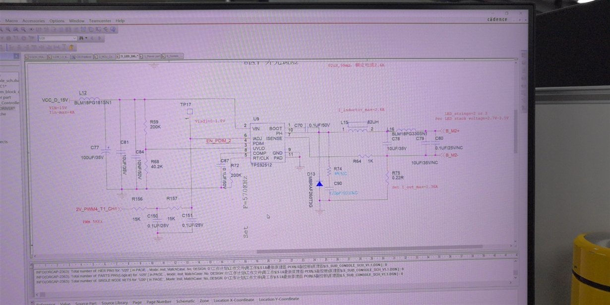
     As shown in he figure,this is the schematic diagram of simulated dimming designed by us. On the same PCB board , we used the same six-way LED driver with the same principle . As the phenomenon desribed 

    before,when Viadj=0,the output current is inconsistent. In the six-way drive,some of the output current is 140mA ,while some of the output current is 50mA or even lower. This is phenomenon is the problem of 

    inconsistent output. IF Viadj=0,I=145mA,when given Viadj an analog volttage ,the output current will superposition the current when the Viadj=0 on the basis of the calculated value. This is error will have a 

    great impact on the product. Therefore, I would like to ask why there is such a big difference in the output current under the same circuit. Please advise

    In addition, we tested the tps92512 demo PCB board when Viadj=0 and Iout =145mA,at this time,each current value on the entire output current curve would be superposition 145mA,resulting in a higher output 

    value of 145mA than the theoretical calculatiion.

    thank you!

  • Hello,

    I don't see 'As shown in the figure', there is no figure.

    It is recommended that the inductor current remains continuous.  From the pin description on page three of the datasheet:  'Analog current adjust pin. The voltage applied to this pin will set the current sense (ISENSE pin) voltage.
    IADJ 6 I The range of the ADJ pin is 180 mV to 1.8 V and the corresponding ISENSE pin voltage is the IADJ pin
    voltage divided by 6."

    What does the circuit going to Iadj look like?  What is your switching frequency?  Do you have a schematic you can share?

    The offset in the error amplifier will not allow accurate dimming at lower levels.  If you are looking for accurate analog dimming to low light levels this is not the part to use.

    8.3.4 Adjustable LED Current (IADJ and ISENSE Pins)
    The LED current can be set, and controlled dynamically, by using the IADJ pin of the TPS92512. Equation 7
    shows the relationship between the voltage applied to IADJ (VIADJ) and the regulation setpoint at the ISENSE pin.
    Equation 8 shows how to calculate the value of the current setting resistor (RISENSE) from the ISENSE pin to
    ground for the desired LED current.  The IADJ pin voltage range is 0 V to 1.8 V and is internally clamped at 1.8 V. If analog current adjustment will
    not be used, the IADJ pin can be connected to VIN through a resistor for a default ISENSE voltage of 300 mV.
    This resistor should be sized so that the current into the IADJ pin is limited to 100 μA or less at the maximum
    input voltage. A precision reference between 0 V and 1.8 V can also be used on IADJ to control the ISENSE
    voltage. If no external voltage source is available, the IADJ pin can be tied to the RT/CLK pin either directly or
    using a resistor divider to generate a voltage between 0 V and 500 mV. If a resistor divider is used off the
    RT/CLK pin to generate the IADJ voltage it will introduce a parallel resistance with the RT resistor. High value
    resistors are recommended in that case and the parallel combination must be used to calculate the switching
    frequency. The current sense voltage is most accurate with IADJ voltages between 180 mV and 1.8 V for a
    dimming range of 10:1. Below 180 mV the TPS92512 dims well but may have more variation between circuits.
    Due to internal offsets pulling IADJ to 0 V will not result in a current sense voltage of 0 V. Some small current will
    continue to run unless the PDIM pin is pulled low or the device is disabled using the UVLO pin. Analog dimming

    is also most accurate when the device is in continuous conduction mode (CCM). If the highest accuracy possible
    is desired during analog dimming, size the inductor so that 1/2 the peak-to-peak inductor ripple is less than the
    minimum LED current to remain in CCM. The IADJ pin should be decoupled with a 10 nF capacitor to ground. A
    1 kΩ resistor should be used between the ISENSE pin and RISENSE to protect the pin in the event RISENSE opens
    or there is a transient due to one or more LEDs shorting.

    Best Regards,

  • hello 

     I'm sorry that the picture was not uploaded successfully.Our design is based on the demo board principle of TPS 92512.

    Here is the re-uploaded schematic.Set the switching frequency at 570 KHz.

    Thank you!

  • user6400890 said:

    hello 

     I'm sorry that the picture was not uploaded successfully.Our design is based on the demo board principle of TPS 92512.

    Here is the re-uploaded schematic.Set the switching frequency at 570 KHz.

    Thank you!

  • Hello,

    Your schematic looks fine, I don't see any issues with it.  For deep analog dimming I would recommend a different part.

    Best Regards,