What do I need to know about dV/dt when designing a driver bootstrap supply?
This thread has been locked.
If you have a related question, please click the "Ask a related question" button in the top right corner. The newly created question will be automatically linked to this question.
Reducing the startup time of a bootstrap supply is often desirable, but increasing the startup speed often leads to unforeseen problems related to dV/dt. Fig. 1 provides an example schematic with the bootstrap resistor, capacitor, and diode highlighted.
Figure 1: Simplified Bootstrap Schematic with Bootstrap Components Highlighted
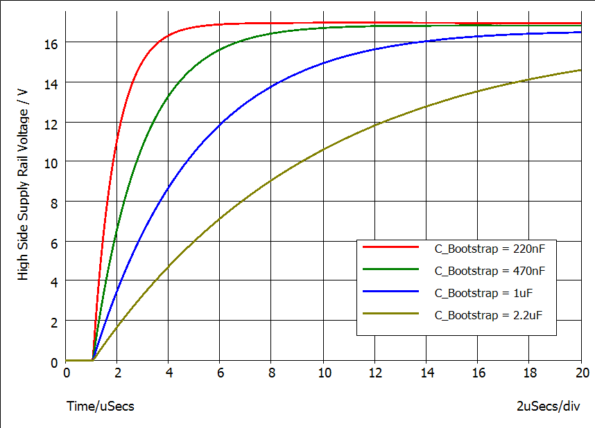
High dV/dt across the bias supply of the driver can have a significant impact on a bootstrap circuit’s function and reliability. This is because large dv/dt spikes can cause high-side FET oscillation, supply overshoot, and gate driver ESD protection cell activation. These results can damage the driver over time. Such dV/dt spikes are most likely to occur during the initial power up of the circuit, as the capacitor charges for the first time, but can also be caused a variety of factors during normal operation, including switch node undershoot, inductance on the bootstrap loop, and bootstrap diode reverse recovery. Fig. 2 shows this dV/dt in the form of a steep rise in voltage from a power up simulation with parasitics.
Figure 2: High Side Supply Rail Voltage Varying Bootstrap Capacitance, Bootstrap Resistance 3.9 Ohm
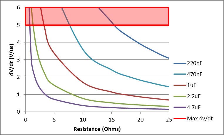
To prevent undesired operation and potential damage to the driver, dV/dt is kept at a reasonable level, with 5V/us being the recommended maximum for the UCC2152x and UCC2122X families. dV/dt can be controlled by increasing the bootstrap capacitor and/or the bootstrap resistor. Fig. 3 plots the dV/dt for various bootstrap resistor and capacitor combinations, clearly marking the acceptable range. For example, if the bootstrap capacitor is 1uF, a bootstrap resistor of at least 3.9 Ohm is recommended.
Figure 3: Peak dV/dt on Power Up when Varying Bootstrap Resistance and Capacitance. (Vdd = 18V)
This procedure will minimize the impact of dV/dt on a bootstrap circuit. If you have further questions about this topic please click the “Ask A Related Question” button and we would be happy to help you.