Because of the holidays, TI E2E™ design support forum responses will be delayed from Dec. 25 through Jan. 2. Thank you for your patience.

This thread has been locked.

If you have a related question, please click the "Ask a related question" button in the top right corner. The newly created question will be automatically linked to this question.

TPS25924: OVP mode detection time

Part Number: TPS25924

Hi,

Let me discuss the OVP mode of TPS25924.
In that evaluation, μsec order ringing is applied to VIN.
I want to know if it is in OVP mode due to this input/output difference.
・Vin:12V ・Iout:≒2A ・Ringing peak voltage: 18V/1μsec

Please tell us about the following contents in the background.

1.Could you tell me the detection time and threshold of OVP mode.

2. Related to question 1, how long does the TPS25924 exceed 10W for thermal foldback control?
    And Could tell me the detailed operation of thermal foldback and the method to confirm whether or not the thermal shutdown has occurred.
    I would like to know the input/output voltage/current waveform and diagram of thermal foldback operation.


I would like to send you a private message about the actual waveform and schematic.

Best regards,
Yusuke

  • Hi Yusuke,

    The response time for the device to start clamping the input voltage can be in the order of 5-10us.

    So, the device would not be able to clamp a 1us over voltage ringing peak.

    The device would foldback the current limit value as and when it measures a power dissipation of around 10W in the Mosfet. This generally happens when the device is limiting the current or clamping the over voltage. 

    The easiest way to know if a device is in thermal stress is to check Vin, Vout and Iin. When there is Iin not equal to 0A and Vin is greater than Vout, there is power dissipation in the device due to current limiting or over voltage clamping.

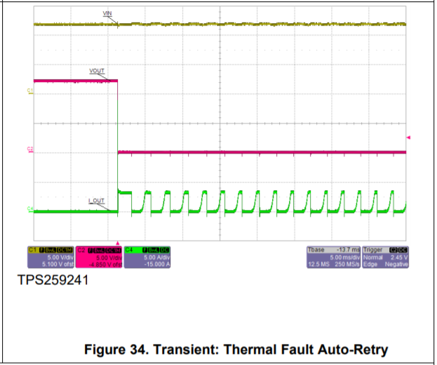
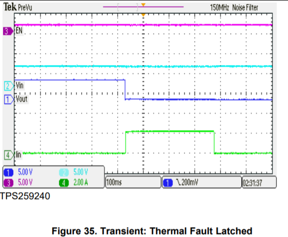
    Figure 34 and 35 in the datasheet show the device turn OFF due to thermal shutdown after limiting current for an output short circuit condition.

  • Hello Praveen,

    Thank you for your response and approving friend request.
    I sent the customer's waveform and circuit information using a private message.
    Would you like to check the wave form?

    Customer wants to know what protection turned off TPS259240.
    It did not turn off at room temperature.
    This OFF phenomenon is measured in the TA=65deg environment.
    However, a voltage transient was confirmed just before turning off.
    Customer would like to know whether Thermal shutdown or OVP mode protection (ISC) is causing the device to be turned off.
    Could you tell me what protection is turned off?

    Best regards,
    Yusuke

  • Hi Yusuke,

    Thanks for sharing the waveforms. From the waveform that you have shared, it seems that the device has turned OFF due to Thermal Shutdown.

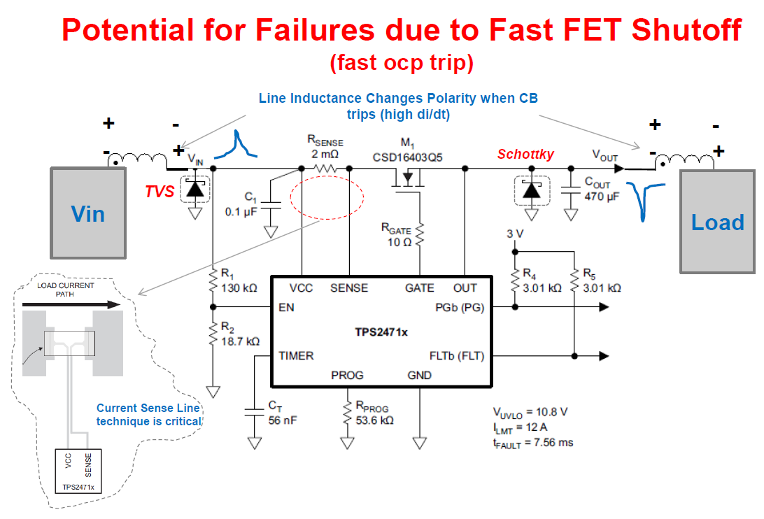
    The Voltage spike that you see on Vin is a consequence of Fast turn OFF. This is possible if there is inductance in the input path. The sudden drop in current flow due to FET turn OFF increases the di/dt and thereby a voltage across the input inductance is generated which adds up to the input voltage and shows up as  a spike on Vin.

    To avoid turn off of the efuse at high temperature, you can try the following,

    • Increase the Cdvdt capacitance
    • Improve layout - reduce RQJA by providing more copper area and cooling to the efuse
    • Reduce the Output capacitance
    • Avoid any load during startup. Apply load after the efuse output is ramped up.