- Ask a related questionWhat is a related question?A related question is a question created from another question. When the related question is created, it will be automatically linked to the original question.
This thread has been locked.
If you have a related question, please click the "Ask a related question" button in the top right corner. The newly created question will be automatically linked to this question.
I need some help for my buck boost design.
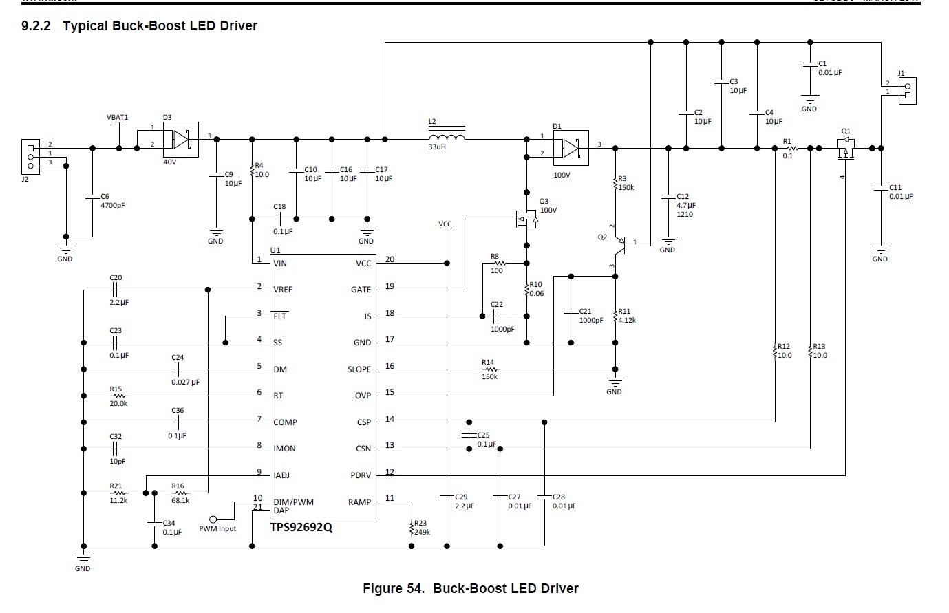
I decided to start set up datasheet's buck boost converter design and then want to see how it works but I can't.
According to datasheet ,I just set up same design and only difference between my design and datasheet is that I didn't want to use DIM/PWM.My purpose is see the constant current without DIM and test the protections of
I placed 10nF to Ramp pin , I connected DIM/PWM pin to Vref(5V) for disable to PWM dimming.
so driver doesn't work,when I check the Gate pin for see the signal which is drive the N-CH MOSFET ,there is no stable frequency.
and then I check the fault detection table
Vcc = 7.5V
Vıs = 1.7mV I guess here is the problem.
Vo = 0.834V
Vcsp-csn = 1mv Also here unexpected value.
Vımon = 14 mV
Vıadj = 0.638 V
Vcomp =1.18V
Vref = 5V
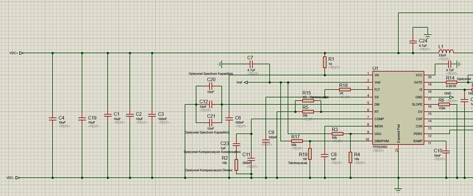
so I put my desşgn schmatic here and I want to help to understand what is wrong with it.


Hello,
The application engineer who will support this question is currently out of office, and will reply when gets back next week.
Thanks
Sumeet
Hello Sumeet Kulkarn
Okey,thanks for your care.
That is fine as well.I'm waiting him to help me.
Hi I wanted to add few additions.
1. I didn't use PVDR PFET,for now I think doesn't need it.
2. I didn't use BJT on OVP, but I measure this pin and it was 0.834V,I think there is no problem.
3. I only want to control led current IADJ pin,it should be constant 500mA and I dont want to use PWM or dim options. So I have connected 5V(Vref) to PWM/DIM (pin10) and then Ramp pin 10 nF.cap used.(pin11)
The other pins are the same as datasheet's configuration.
In the result,I think there is no current flow,leds turn on with10 mA.It seems like no switching and it works at protection area. As I said,I checked gate signal on scope but unstable frequency and signal have viewed.
Hello,
You have PWM/DIM input at close to ground with R19 being 1 OHM. This will set the part into PWM LO which commands it not to drive any current. If you are not using PWM dimming and want to run continuous current then the PWM dimming input needs to be high so please remove R19 and also change also change Rramp to 249K.
The other issue is that you have 1 Ohm in parallel with 20K for Rt. You need to remove the 1Ohm (R15) for it to operate at 390KHz.
Based on the question you are asking I would highly recommend that you follow the data sheet and design equations and design examples.
Thanks Tuan
These 1R are optional resistors,program doesnt allow me place 0R ,sorry I should have explained,real application there is no resistors there.
so
Rt = 20k , 390khz
R17 = 68k for set PWM to high, I measured it 5V coming from Vref. There is no 1R in real application.
Now,I have changed the Ramp Cap 10nF to 249k resistor but nothing change any idea about what can be the wrong?
Hello,
You need to short D2 out...You do not need this diode. You remove the Dimming FET (Q2) so I assume that you have a short across it. Please remove C22 since you do not need this for now and the value is quite high. You mentioned that the VOP (pin 15) measure 0.834V...What is the input voltage from your power supply (VDC+)? What is the voltage measure on D1 Cathode (output voltage)? What is the voltage measured at LED+?
Please send us scope capture of the following signals as power is applied to the part with timebase at about 1-2mS per division. I am looking for signal on the GATE as you power up the part.
CH1 of Scope: Vin (pin 1) please trigger on CH1 rising edge at 6V
CH2 of Scope: SS (pin 4)
CH3 of Scope: COMP (pin 7)
CH4 of Scope: GATE (pin 19)
Thanks Tuan
Hello Tuan
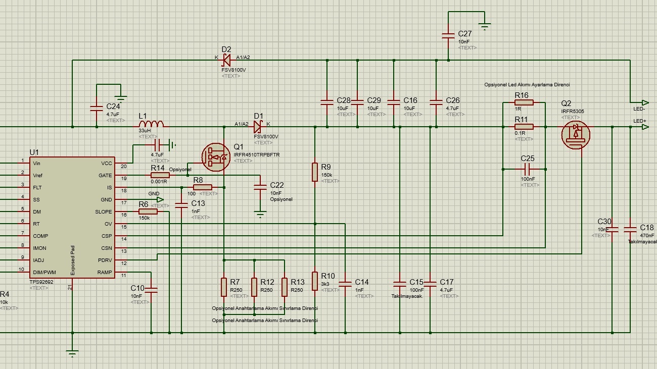
For better conversation, I rearranged my schematic and I just left what I used on PCB.
1- Vin = 17V / Vload = 30V / Iout(rms) = 25mA ( I expecting about 450mA.)
2- I took all of scope captures. (Vin, SS, COMP , GATE).-->> Zip File.
3- The circuit works as it is constantly protecting,but I couldn't find what it is.
Hello Batur,
When you mentioned that Vload is 30V. Is this the LED voltage which is the differential voltage which is Vout - Vin for a Buck Boost or Vout relative to ground is 30V. What is your input voltage range and what is your output voltage LED voltage?
The inductor that you use what is the saturation current and part number?
I notice that you do not have the two 10 Ohm in between R11 and C25 to filter the LED current back to the TS92692. You will need to include this in your design as it is shown the the application Figure 54 of the data sheet.
I notice on the scope capture of SS you have it going below ground. There should not be any voltage on the board that goes below ground.
If you have issue with your board I would recommend that you get a TPS92692 evaluation board to help you with your issue.
Thanks Tuan
Hello Tuan
As you mentioned I have configured the design like application note.
Vin is between [7V to 18V] and Vout = 24 V Iout = 330mA,then, I'm releasing the design schmatic to here.
Circuit works as
1- Vin between [7V to 9V] , no constant current just flickering.
2- Vin between [9V to 16V] ,Iout = 260 mA to 280mA and the Vref falls to 4.2V unexpectedly.
3- Vin between [16V to 17V] ,Iout = no constant current just flickering.
4- Vin between [17V to 18V] ,Iout = about 300 mA.
Note :R8,L3,L4 are ferrit beats., R17 is not used it is optional.
Hello,
Base on your scope capture of SS still going below ground and your not understanding some of the things I mentioned such as there should be no voltage on the board that goes below ground. There is definitely something wrong with your layout and or design.
As I mentioned before...You should obtain an evaluation board to help you with your design.