This thread has been locked.

If you have a related question, please click the "Ask a related question" button in the top right corner. The newly created question will be automatically linked to this question.

LM25085: Vout dropping when loading the buck regulator

Part Number: LM25085


Greetings,

Here's the design with LM25085 regulator designed for a max of 8A Iout at 12V Vout from a pack of 4s Li-Ion batteries. Now we're testing with a power supply set at 16V and current limit of 5A. When connected to a 3Ohm load the Vout droops from 12V to 10.9V and the power supply is only supplying 2.8 A, below its limit of 5A.

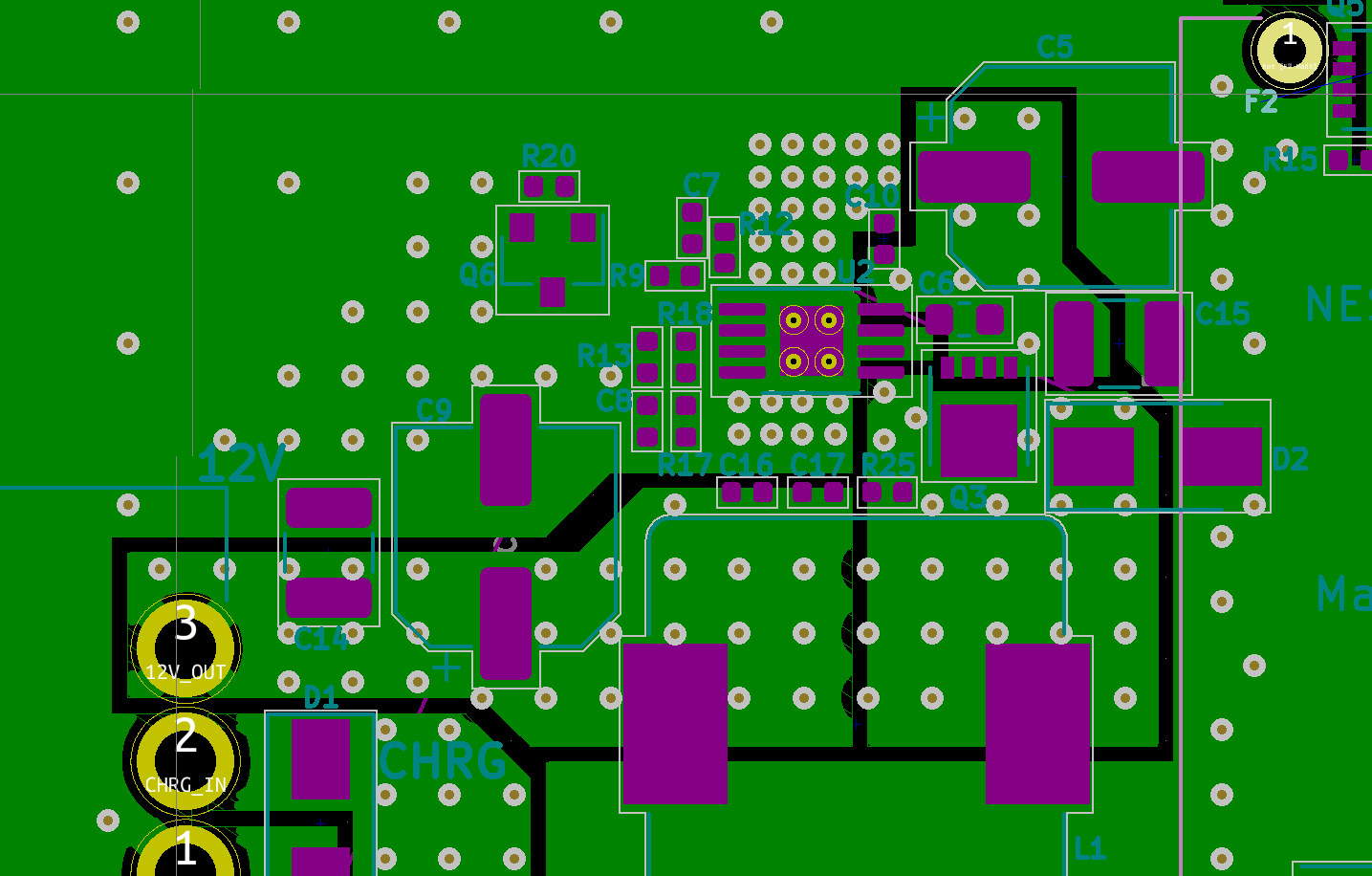
Here's the schematic

And here's the layout

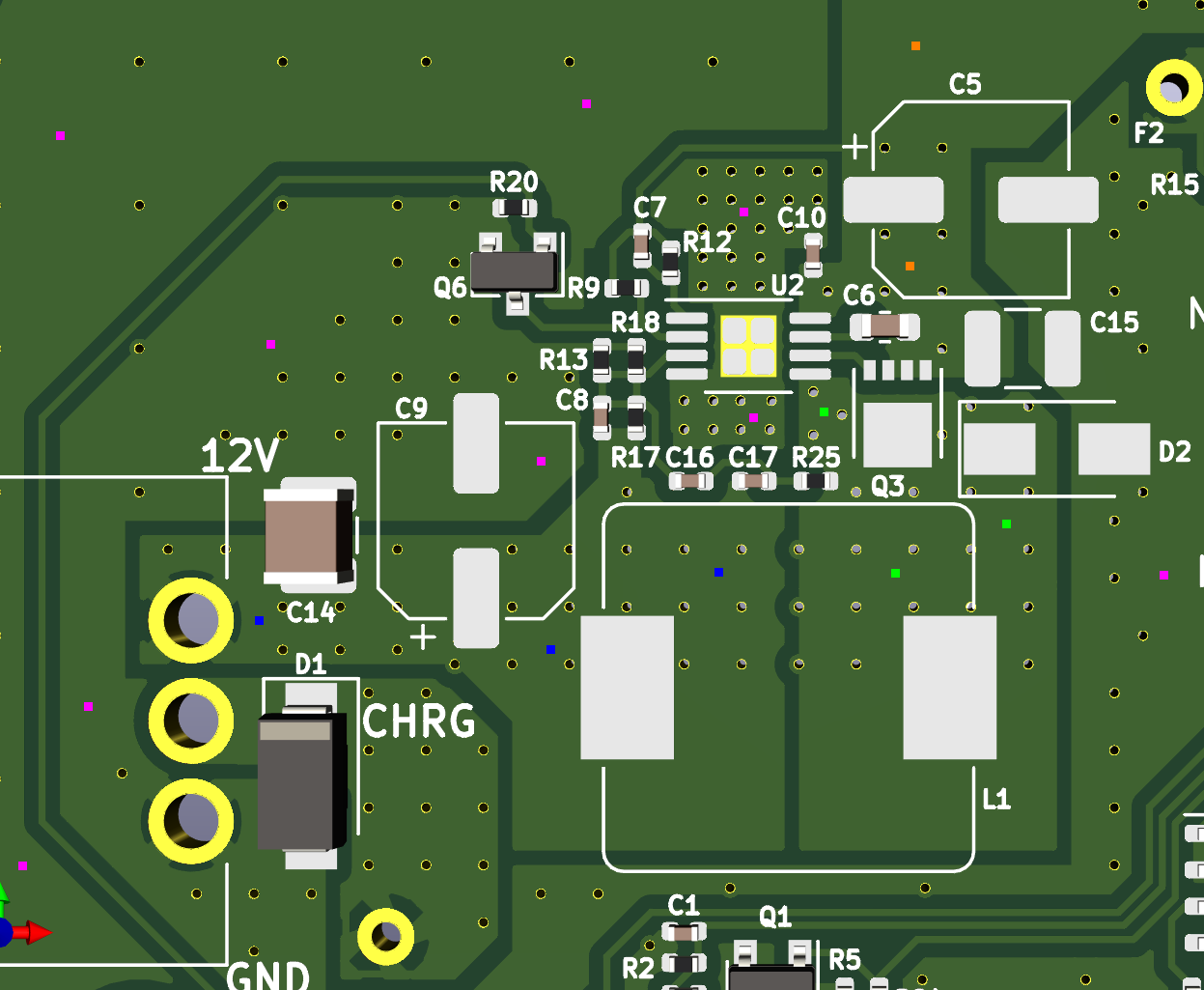
In all the copper pours where there is a via, there is the same copper pour on the bottom layer in this 2 layer 1.6mm PCB. I've put in dots of color to give reference to the nets. Purple is GND, Orange is Vin, Blue is Vout, light green is the net connected to PMOS drain.

In terms of the temperature, the L1 inductor is about 48 C, C9 is 55 C, U2 is 44 C, Q3 is 46 C, C5 is 38 C when running for 15 min driving a 3 Ohm load. Is it throttling because of the heat?

One thought is to increase the Radj from 2.7k (R12) to say 5k to reduce the current limiting. Is this the reason for the Vout drooping? Q3 MOSFET's Ron is at most 17 mOhm, so as per the calculation as per the datasheet, the current limit shouldn't be hit.

Please let us know your thoughts and also any ways to improve the layout.

Thanks, Prithvi

  • Hello

    Here are some thoughts:

    1. The connection from C7/R12 must be made directly to the source of the FET for current sensing.

    You could try to cut the connection you have now, and connect a short wire to the source.

    2. In the end, you still may need to adjust R12 to get the current limit you need, if that is the issue.

    Since the FET Rdson is variable.

    3. Double check you design with the quick start calculator tool on our website.

    4. If you need well defined current limit, then the alternative method of using the sense resistor would be more accurate.

    Thanks

  • Thanks for the quick response Frank.

    We are not concerned about accurate current limit, our load will take an absolute max of 8A, usually at most 5A. We don't need the current limit to be accurate. Even if the current limit is 15A, It is fine.

    For 1. the only issue that will occur with this is that the small length of copper pour resistance would be added to Rds(on), right? This would add 2 mOhm or so at most, right? Even with this the system should work.

    For 2. we changed R12 from 2.7k to 4.7k without any change in the behaviour.

    We have more observations now of the output voltage in different load conditions:

    - no load: 12.002V

    - 1k: 12.051V

    - 100E: 12.629V

    - 15E: 11.697V

    - 7.5E: 10.894V

    This is very strange because there are situations where the Vout is increasing and decreasing according to the load. Any idea why this could be the case?

    Thanks, Prithvi

  • Hello

    It is possible that the device is unstable.

    Check the switching wave-forms during the load testing.

    Also, try disconnecting the trace from the R17/C8 node and

    connected directly to the (+) side of C9/C14.

    Thanks

  • Hi Frank, thanks for getting back to us.

    We did as you suggested - getting the 12V out with a wire from C14 + terminal to the R17 feedback divider. No change in the behaviour

    We also removed R25 resistor that is added to remove the voltage ripple to see if there is any issue it is causing with the feedback but no change in behaviour.

    Here are the waveforms of the switching node in red and the PFET gate voltage input from the regulator (yellow) for different loads

    7.5 Ohm load

    15 Ohm load

    100 Ohm load

    1k load

    No load


    Please note the difference in time base in no load condition. Can you please let us know the reason for the oscillation? Here's the bottom layer with the top layer components. Would switching to a continuous GND layer in bottom layer help? How will the thermal dissipation from the switching node be in that case?

    Thanks, Prithvi

  • Hello

    The ringing you see is just the result of the inductor current ramping to zero and the inductor and parasitic capacitance ringing.

    I am not sure that it is a thermal issue.  However, using more ground plane on the bottom would help with thermals.

    I will ask the application engineer for this device to see if there is anything else we can suggest.

    Thanks

  • Hello Frank,

    Thanks for the response. How would we resolve the drop in voltage at output ?

    Suggestions so far :

    1. The connection from C7/R12 must be made directly to the source of the FET for current sensing. Modify the design

    You could try to cut the connection you have now, and connect a short wire to the source.

    2. In the end, you still may need to adjust R12 to get the current limit you need, if that is the issue.Modify the design

    3. Double check you design with the quick start calculator tool on our website. We generated the circuit using webench

    4. If you need well defined current limit, then the alternative method of using the sense resistor would be more accurate.Modify the design

    Or Do you suggest any more tests to identify the issue ?

    Thanks for your support. Any further support to resolve the issue quickly would be very much appreciated as we running against time for a demo.


    Regards,

    Darshan

  • Hello

    I think that you should try using the calculator to double check the design.

    Webench does not always give a good design.

    The apps engineer for this device suggest that the C8 is not needed.

    Please remove and check values with the calculator and substitute if needed.

    Also, be sure that the inductor is not saturating under load.

    Thanks

  • With the exact values suggested in the Excel calculator, it is working much better. With 3.5A load the output voltage is dropping to only 11.7V, though there are still spikes of +/- 2V in Vout.

  • Hello

    The spikes may be caused by the ESL or ESR of the Al. output cap.  Or maybe the ground routing.  The output cap grounds

    should be near the diode ground with a short route.  Also, the spikes may be coming from your scope probing.  Be sure to probe

    directly across the output capacitor.

    Thanks

  • Hello

    I will close this post.

    You can re-open if you need more help and another

    engineer will be assigned to help you,

    Thanks