This thread has been locked.

If you have a related question, please click the "Ask a related question" button in the top right corner. The newly created question will be automatically linked to this question.

LMG1020: The Vgs is pulled down form 4.8v to 3v when MOSFET turn on

Expert 1055 points
Part Number: LMG1020

Hi Jeffery,

   I encountered a difficult problem these days and want to ask for your help.

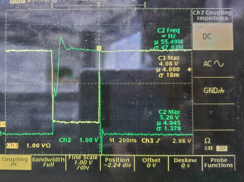
  The problem is like this. As shown in the figure below, I use 1020 to drive epc2022 to control LD (here with LED instead). When R2 is disconnected and Vds is not powered, the driving signal is output at 4.8v after 1020, but when I connect R2  Other conditions are the same as above), the VSW signal amplitude is pulled down to 3v, I also replaced the MOSFET and the 1020 phenomenon is still the same, what do you think is the reason?

  • Hello SUy,

    Thanks for reaching out.

    Can you confirm that VDD (I assume a 5V supply), and INP connections? Can you confirm that R3 is 0-Ohm. 

    With R2 shorted, and no power on VDS (from V2 supply), what do you get at the gate?

    Regards,

    -Mamadou

  • Hi Mamadou,

      Thanks for your reply.

       I use an external 5v power supply for VDD,and the INP input is a pulse signal(4ns,5v,RPF=20khz),I measured the output amplitude of U5 to be 4.7v regardless of whether the MOS tube is turned on or not. The R3 i confirmed,it is 0-ohm.

      When R2 shorted, the gate drive signal is always pulled to 3v Regardless of whether there is VDS.

      I found that when the trigger pulse width is very narrow, the Vgs amplitude will be very low. The following figure shows the waveform of Vgs when the driving pulse width is 100ns and 500ns.But I still can’t understand why Vgs rises so slowly. Could it be a problem with my layout? (Green is the Vgs waveform, yellow is the drive signal)


    My real circuit is like below:

  • Hello SUy,

    Thanks for the details.

    As you know, inductance the circuit will certainly impact the signals. Depending on where the inductance is coming from, you might have much slower edges and/or ringing. We typically recommend very short connections using thick traces as PCB inductance is inversely proportional to trace length and width. 

    My colleague discusses how to minimize layout related parasitic on the attached application note.

    https://www.ti.com/lit/an/slla456/slla456.pdf

    Another thing to check/consider is as sanity check, you may try to look at VSW test point then comparing to driver IC OUT rise/fall times directly at the pin to confirm how much difference/delay the (0-ohm resistor I assume you're using 0402 resistors) and trace inductance from driver OUT to gate is introducing in your circuit.

    Please let us know if you have additional questions.

    Regards,

    -Mamadou

  • Hi Mamadou,

        Tnaks for your reply.

        I think my PCB trace cause the raising edge of Vgs to slow down,so i will change my routing.