This thread has been locked.

If you have a related question, please click the "Ask a related question" button in the top right corner. The newly created question will be automatically linked to this question.

BQ76952EVM: BQ76952 EVM showing PCHG and PDSG showing 1.7V difference while toggling

Part Number: BQ76952EVM
Other Parts Discussed in Thread: UCC27524

HI,

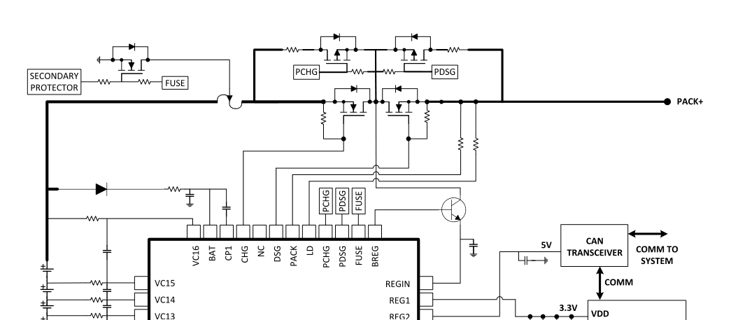
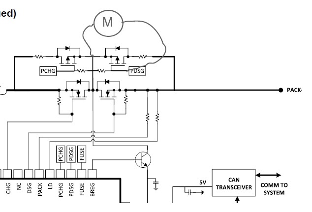
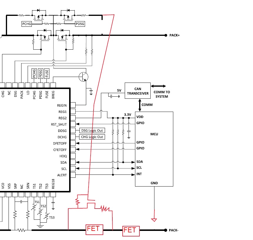
I was trying to check Voltage output at respective FET pins of EVM board and following are my findings:

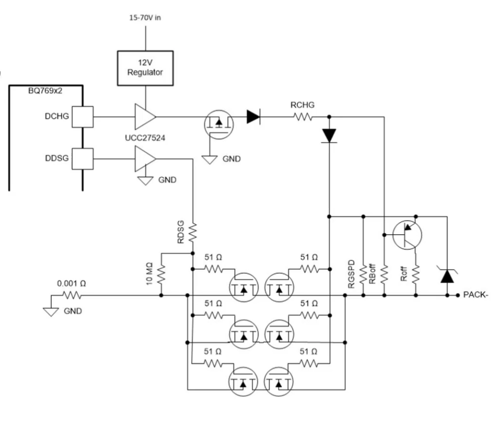
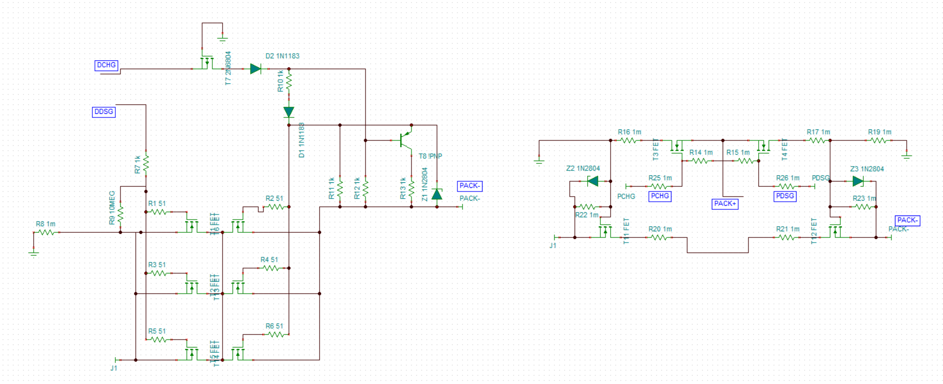
  • CHG shows 64.2V / 53.3V
  • DSG shows 64.8V / 0V
  • PCHG shows 46.2V / 44.5V
  • PDSG shows 46.2V / 44.5V
  • DDSG and DCHG shows 5.25/0V

Although, I understand CHG, DSG, DDSG and DCHG outputs.

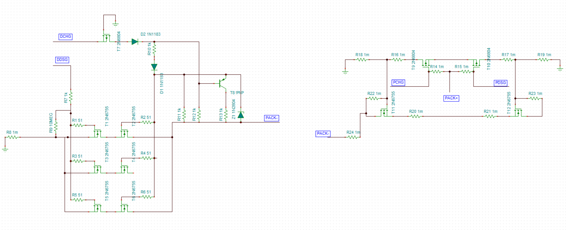
I am unable to understand PCHG and PDSG voltages, as datasheet states this:

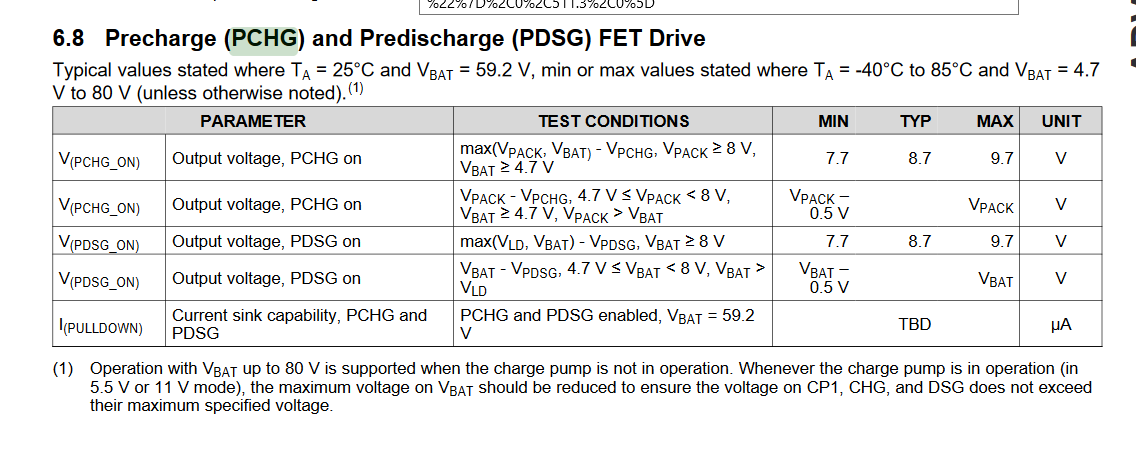
I am planing to use a low side configuration for FET driving, I know how to use DCHG and DDSG for driving FETs in low side configuration, but I need some clarity on PCHG and PDSG in this regard.

Regards,

Anurag

  • Hi Anurag,

    PCHG and PDSG are pulled down weakly when "on" and high impedance when "off".  When off it is the RGS installed at the FET which turns off the FET.  Measuring the pin voltage with respect to GND/VSS will pull down the pins showing a value typical of your readings.  A high impedance meter will show slightly better result, measuring from BAT to the pin will give a better indication of performance.

    To use pre-charge and pre-discharge for low side connect P-ch signal FETs with the source at the battery voltage.  Rather than switching a power current take the current to a resistor at the low side to control a N-ch FETs for pre-charge and pre-discharge current.  Limit the current in the signal paths as desired, use zeners if needed to protect the gates.

  • Hi,

    Thanks for your reply, I see that you have suggested to measure voltage across BAT to pin, but BAT ground and Board ground is on same level, so Is It gonna make any difference. Although, I get the idea of high impedance meter (I am using FLUKE 17B+).

    As for Low-side drive I am unable to visualize this circuitry, can you help me with reference to the following circuit:

    As far as I understand, you are suggesting to use P-ch FET to drive N-ch FET by adding one resistor and doing required changes.

    Regards,

    Anurag

  • Hi Anurag,

    Yes, measure across the G-S resistor.

    For the high to low transition, you might do something like this, add diodes to block or limit voltage as needed.

  • Hi,

    Thanks for your elaborate reply.

    So, I have created following circuit according to TI resources for low side and your reference:

    Can you please verify it, although I still need to put correct resistor values.

    Regards,

    Anurag

  • Hi Anurag,

    The power FET section seems OK although the charge FETs look reversed and you may want to connect all the drains together so the FETs share current as well as possible.  Also remember that the DDSG and DCHG are 5V max, so select logic level FETs or use a driver with higher voltage supply.  You may want to use Schottky diodes  in the charge gate control if you have the low drive voltage.

    In the precharge/discharge circuit the sources of T9 and T10 will need to connect to PACK+ also.  You may want some resistance to the PCHG and PDSG pins to isolate them from any transient through the FETs.  T11 and T12 look reversed (source & drain).  T12 source needs to connect to the sense resistor.  The common connection of R20 and R21 might go to the common drain of the power FETs unless you want to use all the resistors to limit current & spread power.  R18 is undesired as it will bypass the FETs and sense resistor with a resistive path. It is R22 which will develop the gate voltage for T11, consider if you need a zener across it since PACK- has a large voltage range.  Also R24 seems unusual.  Often a resistor or resistor array at R20 provides current limit, but use a circuit which suits your needs.   

  • Hi,

    Thanks for pointing out these, I was trying to simulate it.

    Another thing I is how should I figure out passive values like RDSG and RCHG or should I refer to datasheet?

    And can you please explain to me what is use of transistor placed on PACK-

    Regards,

    Anurag

  • Hi Anurag,

    RCHG and RDSG will help slow the switching of the FETs to avoid an excessive inductive spikes from the battery or system when DDSG or DCHG switch.  A dedicated FET driver such as UCC27524 is usually very fast.  RDSG for turn off of the discharge FET is usually the main concern since discharge currents may be high, including short circuit.  Turn on is usually less of a concern.  RDSG may need to be tuned for the system to select a value which turns off quickly enough for the FETs used while turning off slow enough to avoid a large inductive spike from the battery.  A value of 1-5 kohm may be an appropriate starting value depending on the FETs used.  The charge path current is often lower current and turn on is again a low concern.  Since the driver can't go above its supply, turn off of the charge FET is accomplished by RDSPD, possibly aided by the PNP and Roff which will provide current gain.  If charge current is low and a modest DC current is acceptable from the driver into RGSPD, a small value for RGSPD may provide an adequate turn off.  For batteries with higher  charging currents the current gain provided by the PNP helping the FETs turn off may be desired.


  • Hi,

    This is really helpful to understand the circuit.

    I have improvised the circuit as following:

    I have been trying to simulate the circuit in TINA TI.

    Can you give me some pointers on how should I verify its working or simulate it, I have been trying to provide 12V at DCHG and DDSG pins as UCC27524 is missing in the circuit.

    Regards,

    Anurag

  • Hi Anurag,

    Simulating with 12V or 0V for the driver output at the DDSG and DCHG nodes on the schematic seems reasonable.  You can simulate a battery with a load resistor to PACK- or charger supply to PACK-, or just put a supply between GND and PACK- and change its polarity.

    The simulation tool people should have experts with advice on simulation if you post a question for the simulator (and the question is for the simulator rather than the BMS product).