This thread has been locked.

If you have a related question, please click the "Ask a related question" button in the top right corner. The newly created question will be automatically linked to this question.

TPS40170: Damaging low-side FETs

Part Number: TPS40170
Other Parts Discussed in Thread: CSD19537Q3

We are seeing some strange behavior with our TPS40170.  Without going into all the detail about what we’ve seen and tried at first, I’m going to try and hit the main relevant (at least what we think are relevant) points:

Overview:

  • We are using the TPS40170 as an adjustable buck regulator by adjusting Vtrk
  • We are using 48Vin as our input, and want to vary the output between ~5V and ~40V out.  Max current is <1A
  • The output is adjusted relatively slowly – our RC filter on the Vtrk input has a time constant of ~10ms, and our SW limits the Vtrk change to a max of ~23mV every 50ms.

Issue:

  • Sometimes, our low-side FET is being damaged: gate, drain, and source are all shorted together.
  • We don’t understand what is causing this – we have been unable to measure any overvoltage condition on the switch node or the gate of the FET so far.

Ideas:

  • Aside from slight ringing, we have yet to measure any kind of overvoltage on the FETs gate pin (high or low side) nor the SW node.
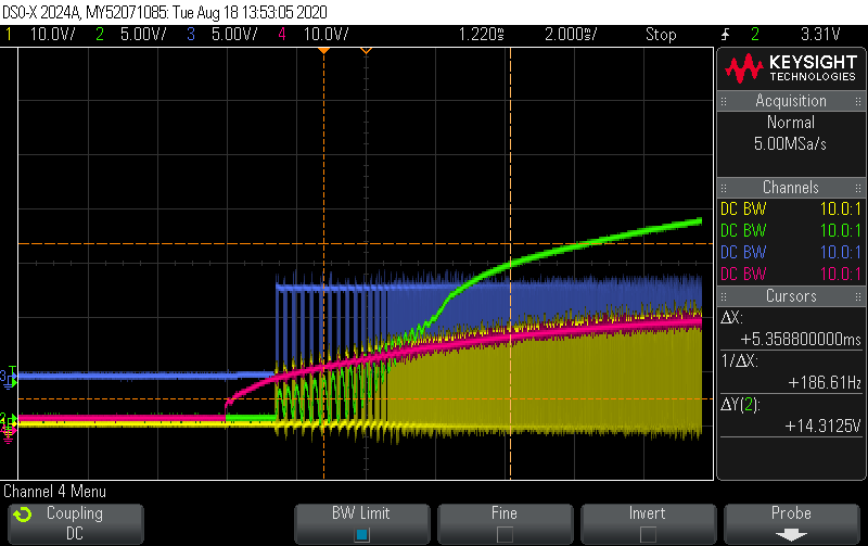
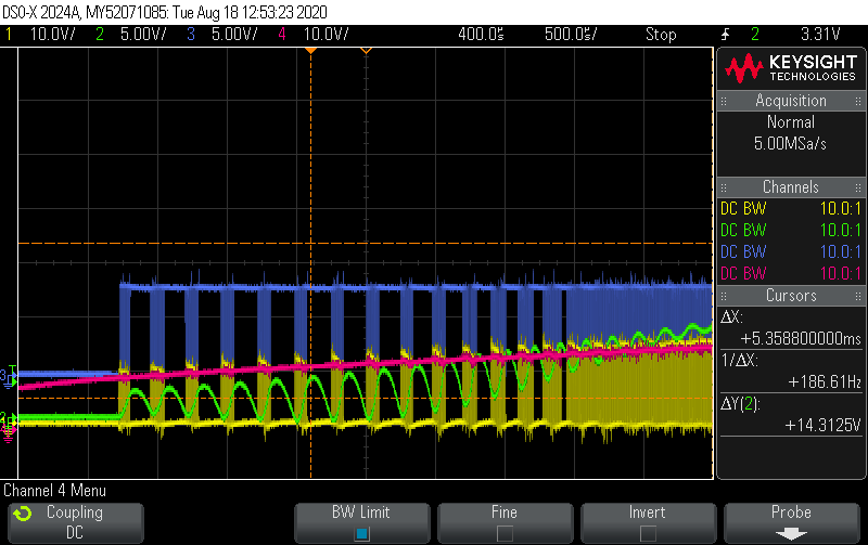
  • We think we have caught some odd behavior of the TPS40170 upon startup (see scope shots below - the second is just zoomed in on the oscillations of the first).

      • Yellow = SW node, Blue = low-side FET gate pin, Green = output voltage, Red = input voltage
    • It looks like the supply tries many times (much more than 7, so I don’t think it’s overcurrent) to start regulating.  But during each attempt, it turns the low-side FET on for ~200us after the output rises to ~5V, which takes the output voltage almost to 0.  Every successive “attempt” makes the output voltage rise to a slightly higher maximum, until it looks like something finally kicks in and it behaves normally and regulates normally.
    • If this were to happen with more than just 5V on Vout, it would surely damage the low-side FET.  With just this 5V output, we are looking at ~40A pulled into the FET during that 200us.  At higher voltages, I can easily see this issue causing the FET to dissipate on the order of 100mJ for each “attempt”.
    • I can’t find anything in the datasheet that would explain this startup behavior.

  • We also would like to understand what the datasheet means by: “For proper tracking using the TRK pin, the tracking voltage should be allowed to rise only after SSEAMP has exceeded VREF, so that there is no possibility of the TRK pin voltage being higher than the SSEAMP voltage”.  Since we are using the TRK pin to adjust our output voltage, what should we do with it during startup / error conditions?

Thanks in advance for the help!

-Bill

  • Hello Bill,

    Can you please send the schematic and layout.

    Also what is the part number for the low side FET that you are using? According to the datasheet:

    'If the low-side MOSFET has low gate

    capacitance CGS (if CGS<CGD), there is a risk of short-through induced by high dv/dt at switching node (See

    reference[1]) during high-side turned-on. If this happens, add a small capacitance between LDRV and GND.' (pp. 29)

    So in the mean time try adding this small capacitance between LDRV and GND and see if this helps solve the low side FET issue.

    In terms of your question regarding TRK voltage:

    The output voltage is regulated so that the FB pin equals the lowest of the internal reference voltage (VREF) or the level-shifted SS pin voltage (SSEAMP) or the TRK pin voltage. So if you want to use TRK pin to set the output voltage, it must be between 0 and 600mV. The time it takes the SSEAMP voltage to reach VREF=0.6V is defined as the soft start time tss, this is set by the soft start capacitor and can be calculated using equation 10 in the datasheet. By holding TRK low until after the soft start time, and ensuring that the maximum slew rate of the TRK pin voltage is less than the bandwidth of the system it is assumed that the rise time of the TRK voltage will not exceed that of the SSEAMP ramp and will therefore never go beyond 600mV. Therefore it can be used to establish the output.

    Sorry for the wordy response but I hope you find it helpful.

    Regards,

    Harrison Overturf

  • Harrison,

    From looking at the gate drive signals directly on both FETs, there seems to be ~500ns of dead time - I don't think shoot-through is happening - at least not in the normal condition.

    The FET P/Ns are:

    • High Side = CSD19537Q3
    • Low Side = BSC340N08NS3G

    Regardless, we have seen the issue (damage to the low-side FET) both with a 1000pF cap on its gate (LDRV pin) and without.

    As for TRK, do you think holding TRK to ~60mV through startup is low enough?  Without modifications to the board, that is the best we can do.

    Do you have any insights into the weird behavior we've captured at startup?  I can tell you that the TRK pin as steadily increasing during that time.  The datasheet mentions that the regulator has a state machine in it, but doesn't go into any details about the state machine.  I wonder if we're accidentally getting into some weird state.  Thoughts?

    And as for my schematic / layout - I can share it with you over email, but not over a public forum.  How can I email you?

    -Bill

  • Bill,

    I'm going to close this thread and we can continue this offline.

    Email me here:

    h-overturf@ti.com

    -Harrison