This thread has been locked.

If you have a related question, please click the "Ask a related question" button in the top right corner. The newly created question will be automatically linked to this question.

UCC28950: ZVS operation , Miller Clamp

Part Number: UCC28950

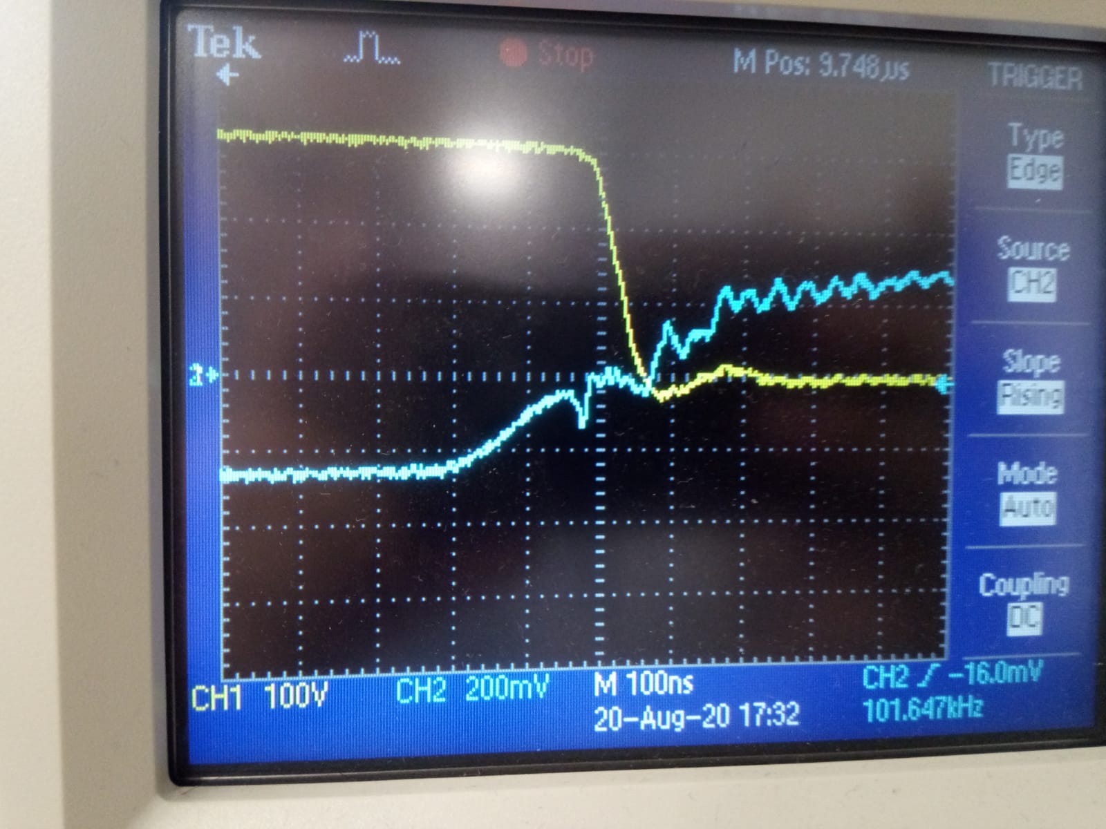
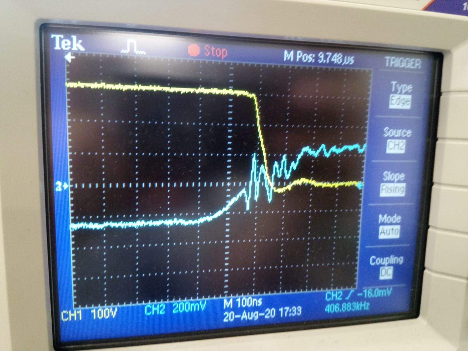
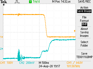
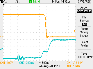
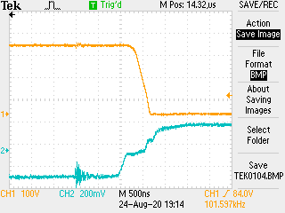
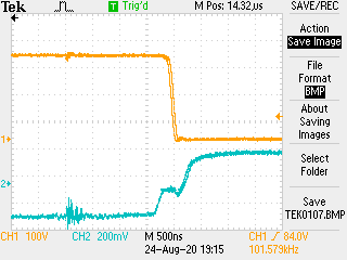
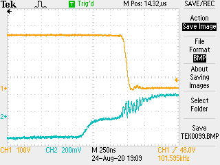
Hello Team , There are 3 different cases in the picture as you see below.

Yellow Channel D-S
Blue Channel G-S

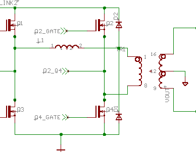
My question is why the miller effet so obvious is?
and does the ZVS achieve i could not understand cause of the miller effect.

1. Picture %35 Load , 2.Picture % 70 Load , 3.Picture %95 Load 


Thanks in advance 

Mikail Ünal


  • suggestions please?

  • Hello,

    There is possible two issues that are not allowing you to ZVS.

    1. Your shim inductor (LS) is not enough to provide energy to achieve ZVS.
    2. Your turn on delay for A and B and C and D switches are not setup correclty.

    The following link will bring you to an application note that describes how to properly size LS and adjust the delay timing to achieve ZVS from 50% to 100 load.  

    The following link will also bring you to an excel design tool that can be used to double check your LS and delay timing.  Please note that initial timing is based on theoretical values and the design always needs to be fine tuned. 

    file:///C:/Users/a0799388/AppData/Local/Temp/sluc222d.zip

    Regards,

  • Hi Mike thank you for the feedback and suggestions.

    I've do new tests and my new results:

    1. picture is the placement of my mosfets.(Sch)
    2.,3.,4.   are the pictures of the Q4 switching element.
    5.,6.,7.   are the pictures of the Q2 switching element.
    8.,9.,10. are the picture of the Q1 (Q3 is similer)

    I've set my Ls like in the calculations also ı've verified with power stage design tool.
    tabset , tcdset are also calculated.

    My opinion is that only Q4 and Q2 is in the ZVS operation like the pictures below , am I wrong?
    but still Q1, And Q3 do not achiving ZVS even in full load.
    and also there is a curve on the top of the drain waveform of the Q1-Q3 switches , what do you think. 

    Thank you

     
    Best Regards 

    Mikail Ünal

    1.Sch

    2.Q4


    3.Q4

    4.Q4


    5.Q2

    6.Q2


    7.Q2 


    8.Q3-Q1


    9.Q3-Q1


    10.Q3-Q1


  • Hello,

    Please note the CD FETs in a phase shifted full bridge achieve ZVS earlier that AB FETs because they have reflected output current to help transition the switch node.   The following link will be you to 600W reference design.  Figure 10 through 15 show how the switch node behaivor changes with current. 

    When designed per the application note that was sent you should have ZVS to at least 50% load on the AB switch node by properly selecting Ls.

    I reviewed your waveforms and have the following comments.

    3.Q4, 4.Q4, 6.Q2, 7.Q2 and 8.Q3-Q1  look to have ZVS.  Q2 and Q4 are your C and D driven FETs.

    Wave forms 9.Q3-Q1 and 10.Q3 Q1 are not ZVS, these are your AB driven FETs.

    1. The turn on delay should be set so they valley switch.  It looks like the turn on delay should be 250 ns. 
    2. I would try fine tuning the delay to achieve valley switching on these nodes.
    3. I would also try increasing the Ls inductor so there is more energy to achieve ZVS over a wider load range.

    Regards,

  • Thank you for you suggestions expert! i will try again thank you soo much.