This thread has been locked.

If you have a related question, please click the "Ask a related question" button in the top right corner. The newly created question will be automatically linked to this question.

TPS40211-Q1: TPS40211QDGQRQ1 Not Switching

Part Number: TPS40211-Q1
Other Parts Discussed in Thread: TPS40210-Q1

Hello,

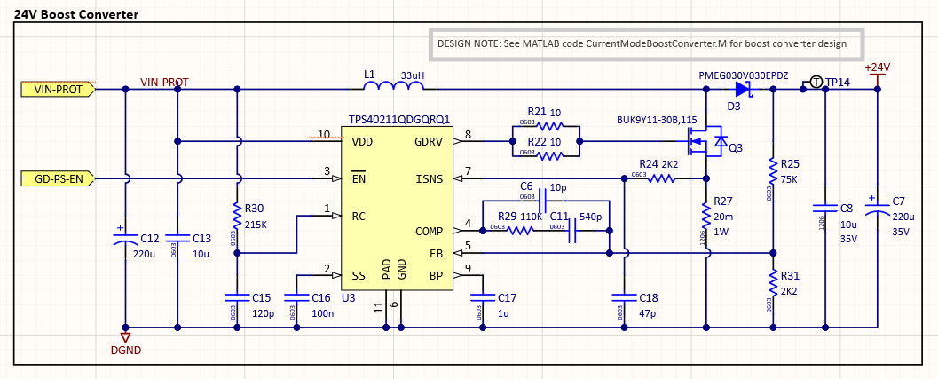
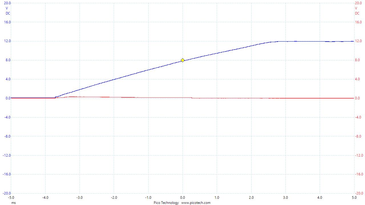
I'm using the TPS40211QDGQRQ1 in my boost converter design to go from 8V - 16V to 24V. I'm running into an issue where Vout = Vin - V_diode. That is, the switcher is not switching. There are no gate signals being generated. The nEN is disconnected so the internal pulldown is pulling it low. I have verified a DMM that this node is 0V.

I've checked my design a few times using the 8.2.2 Detailed Design Procedure in the datasheet, but haven't had any success. I thought it might be my compensation network, but would this cause the switcher to not switch at all?

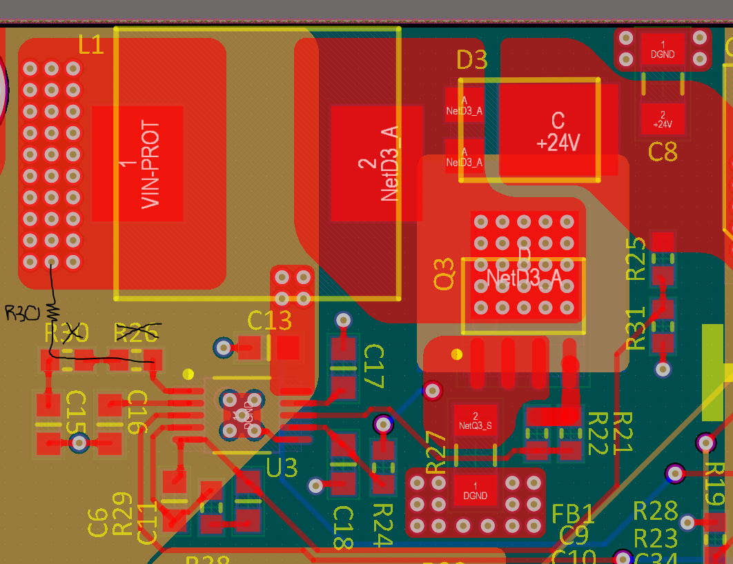
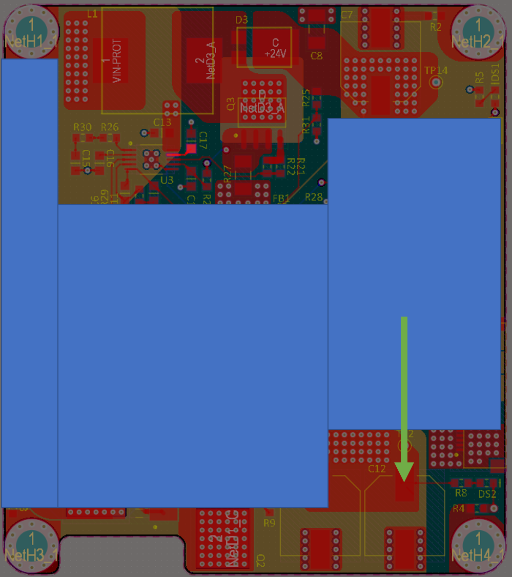
My schematic and layout are shown below. Thank you for the support.

J

  • Also this is the MATLAB code I refer to in the schematic 


    clear
    clc
    
    %% Duty Cycle
    Vinmin = 8;  % Boost converter minimum input voltage [V]
    Vinmax = 16; % Boost converter maximum input voltage [V]
    Vout = 24;   % Boost converter output voltage [V]
    Vfd = 0.5;   % Forward voltage drop of diode [V]
    
    Dmin = (Vout - Vinmax + Vfd)/(Vout+Vfd); % Minimum duty cycle
    Dmax = (Vout - Vinmin + Vfd)/(Vout+Vfd); % Maximum duty ratio
    
    %% Oscillator - Switching Frequency
    fsw = 600 * 1000; % Boost converter switching frequency [Hz]
    Ct = 120;  % Oscillator capacitor [pf]
    
    Rt = 1 / (5.8e-8 * (fsw/1000) * Ct + 8e-10 * (fsw/1000)^2 + 1.4e-7 * (fsw/1000) - 1.5e-4 + 1.7e-6 * Ct - 4e-9 * Ct^2);
    % Required oscillator resistance [kohm]
    
    %% Inductor Selection 
    Iout = 1; % Boost converter output current [Amps]
    Vin = 12; % Nominal input voltage [V] 
    D = 0.5;  % Duty ratio where worst-case current ripple occurs
    
    I_lripmax = 0.3 * (Iout / (1 - Dmin));
    Lmin = ((Vinmax / I_lripmax) * Dmin * (1 / fsw)) * 10^6; % Minimum inductor size in uH
    
    L =  33 * 10^-6; % Selected inductor [H]
    
    Iripple = (Vin / L) * D * (1 / fsw);
    Iripplevinmin = (Vinmin / L) * Dmax * (1 / fsw);
    
    Ilrms = sqrt( (Iout/(1-Dmax))^2 + (1/12 * Iripplevinmin)^2); % RMS inductor current
    Ilpk  = (Iout / (1 - Dmax)) + ((1/2)*Iripplevinmin); % Peak inductor current
    
    DCR = 75.4 / 1000; % DC resistance of selected inductor [ohm]
    Pl = Ilrms^2 * DCR; % Inductor power loss [W] 
    
    %% Rectifier Diode Selection
    
    Vbrmin = Vout / 0.8;  % Reverse breakdown voltage of diode [V]
    Vf = 0.5;             % Forward voltage drop of diode [V] 
    
    Pdmax = Vf * Iout;    % Power dissipation of diode [W] 
    
    %% Output Capacitor Selection 
    Vrip = 100 / 1000; % Output voltage ripple [Vpp]
    Cout = (8 * ((Iout * Dmax) / Vrip) * (1 / fsw))* 10^6; % Minimum output Capacitance [uF]
    ESRout = (7/8 * (Vrip / (Ilpk - Iout))) * 1000; % Output cap ESR [mohm]
    
    %% Input Capacitor Selection 
    Vinripple = 20 / 1000; % Input voltage ripple [V] 
    
    Cin = (Iripple / (4 * Vinripple * fsw)) * 10^6; % Input capacitance [uF]
    ESRin = Vinripple / (2 * Iripple) * 1000;  % Input cap ESR [mohm]
    
    %% Current Sense and Current Limit
    Vocpmin = 110 / 1000; % Overcurrent protection voltage [V] DS constant?
    Idrv = 0.5; % Gate Drive Current [A]
    
    Risns1 = (Vocpmin / (1.1 * Ilpk + Idrv) ) * 1000;  % Maximum current limit requirement [mOhm]
    Risns2 = ( (Vinmax * L * fsw) / (60 * (Vout + Vf - Vinmax)) ) * 1000; % Stability requierment [mOhm]
    
    Rsns = 20 / 1000; % Selected sense resistor [Ohm]
    Psns = Ilrms^2 * Rsns; % Sense resistor power dissipation [W]
    
    %% Current Sense Filter
    Riflt = 2200; % Resistor for RC filter [Ohm]
    Cifltmin = (0.1 * Dmin)/(fsw * Riflt) * 10^12; % Min capacitor for RC filter [pF]
    Ciflt = 47 * 10^-12; % Selected capacitor for filter [F]
    fi = (1 / (2 *pi * Riflt *Ciflt))*10^-6; % Cutoff frequency for filter
    
    %% Switching MOSFET
    
    %% Feedback Divider Resistors
    Vfb = 0.7; % Feedback voltage DS constant [V]
    Rfb = 75 * 1000; % First resistor in divider [Ohm]
    Rbias = (Vfb * Rfb) / (Vout - Vfb) / 1000; % Second resistor in divider [kOhm]
    
    %% Error Amplifier Compensation
    f = 30 * 1000; % Gain crossover frequency
    Ioutmin = 0.1; % Minimum current [A]
    
    Rout = Vout / Ioutmin;
    
    Resr = 160 / 1000; % ESR of electrolytic capacitor [Ohm]
    %Rout2 = 2 / 1000; % ESR of ceraminc capacitor [Ohm]
    %Resr = ((Rout1 * Rout2) / (Rout1 + Rout2)); % Parallel resistance of output capacitors [Ohm]
    
    % Transconductance [S]
    gm = (0.13 * sqrt(L * (fsw/Rout)) / ( (Rsns^2) * (120 * Rsns + L * fsw)));
    
    % Maximimum output impedance [Ohm]
    Zout = Rout * sqrt((1+(2*pi*f*Resr*Cout)^2)/(1+((Rout)^2 + (2*Rout*Resr) + (Resr)^2) * (2*pi*f*Cout)^2))
    
    Kco = gm * Zout; % Modulator gain 
    Kcomp = 1 / Kco;
    R4 = (Rfb * Kcomp)/1000 % R4 [kOhm] 
    
    % INPUTS
    R4_s = 110 * 1000; % R4 selected [Ohm]
    
    % Place zero at 1/10 the desired crossover frequency (fl)
    C2 = (10 / (2*pi*f * R4_s))*10^12; % C2 [pF]
    
    % Place a high frequency pole at about 5x desired cross-over frequency and
    % less than 1/2 unity gain bandwidth of error amplifier
    C4 = (1 / (10 * pi * f * R4_s))* 10^12; % C4 [pF]
    
    GBW = 1.5 * 10^6; 
    C4_BW = (1 / (pi * GBW * R4_s))*10^12; % C4 must be larger than this. 
    
    %% Soft Start Capacitor
    Tss = 5 / 1000; % soft start time [sec]
    Css = (20 * Tss * 10^-6) * 10^9; % SS capacitor [nF]


  • Hello J,

    The compensation can cause a converter not to work at all, so please check these values:

    C6 = 820pF

    C11 = 22nF

    R29 = 15.4 kohm

    A layout could cause such a behavior as well.

    Please explain: What is the basis of your mathlab file?

    Another possibility would be that you review this reference design: 

    This seems to be very close to your requirements.

  • Hi Brigitte,

    Thank you for the feedback. I will replace the compensation network and report back if that solves it. Components will arrive in 3 days. 

    If that doesn't work, I will try to align my design with the reference design. Thank you for sharing that. 

    My MATLAB script is based on the 8.2.2 Detailed Design Procedure in the TPS4021x-Q1 datasheet

  • Hi Brigitte,

    I replaced the compensation network with suggested components, but still got the same result - no switching

    Any other suggestions? I tried on another board and still had no success. 

    Is there anything i can measure for you to help us better understand the problem?

    Thanks

  • Hello J,

    Please check in detail what happens on the different pins when you apply VIN and keep EN low and how this changes when EN gets high. You would need to check this with a scope.

  • Hi Brigitte,

    Attached is a PDF that shows the startup characteristics of each pin when EN is disconnected (pulled LOW). Hopefully there is some useful insight we can draw from this.TPS4021x-Q1 Startup Scope Shots.pdf

  • Hello J,

    I am not able to locate C12 in your layout. Where do you have this capacitor? What is the bandwidth limit of the scope you used? Would it be possible to get a higher resolution picture of the GDRV at the moment when the IC is connected to VIN?

  • Below is an image showing the locating of the bulk capacitor. Because it's a electrolytic bulk capacitor, its my understanding that location in layout was not critical so I put it where there was room. There is a ceramic 10uF (C13) up near the boost converter section.

    Here is the GDRV line at 2 GS and 12 bits of resolution.

  • Hi Brigitte,

    Any other suggestions? I'm baffled. 

    The one thing I am unfamiliar with is the compensation network design so that's what I suspect the issue is but I don't know how to correct it. 

  • I think I know what the issue is. I'm using the TPS40211-Q1. The design guide I followed is for the TPS40210-Q1.

    The TPS40211-Q1 ref voltage is 260mV. The TPS40210-Q1 ref voltage is 700mV. 

    I will correct for this and report back with results. 

  • Hello J,

    Thank you for the update and sorry for no answer for some days, I was out of the office.

  • I changed R31 to 820 ohm and the compensation network to the values you initially recommended

    C6 = 820pF

    C11 = 22nF

    R29 = 15.4 kohm

    That solved it. Thanks for your help Brigitte!