This thread has been locked.

If you have a related question, please click the "Ask a related question" button in the top right corner. The newly created question will be automatically linked to this question.

LMG1210: Synchronous Bootstrap circuit - calculation of passives

Part Number: LMG1210

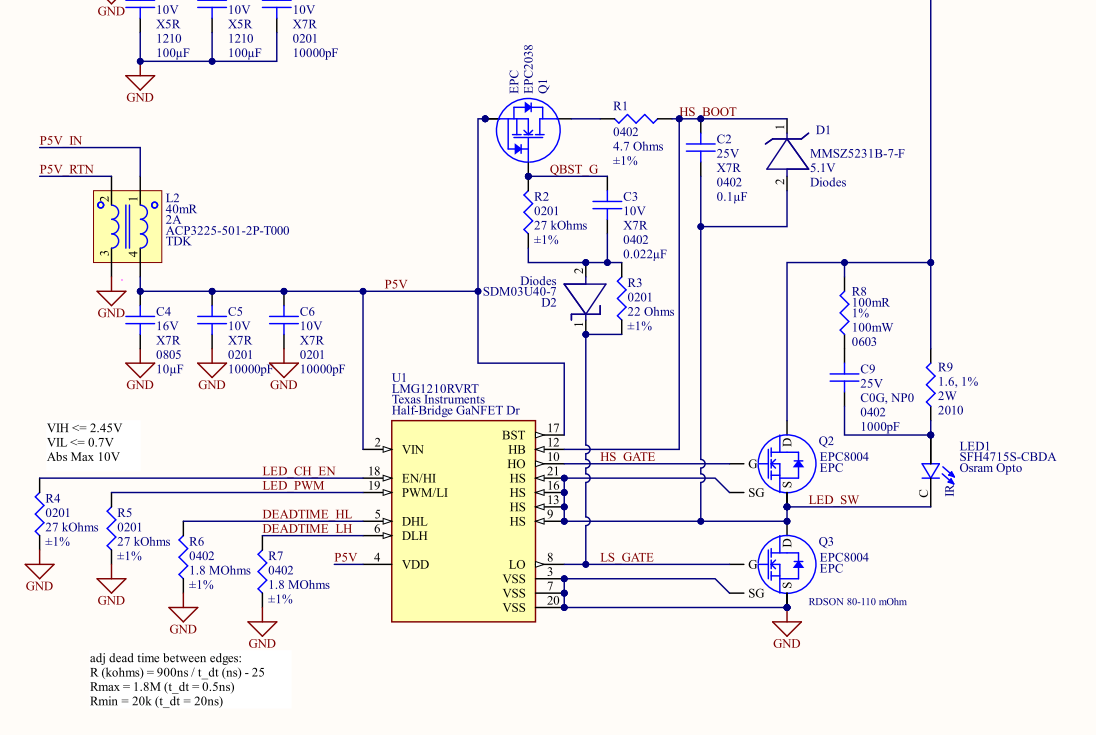
I have just received a board I designed that uses the LMG1210 with the synchronous bootstrap circuit shown in https://epc-co.com/epc/Portals/0/epc/documents/schematics/EPC9066_Schematic.pdf.  This is the same circuit that is referenced in the answer to this support question.  

I want my rise and fall time to be less than 5ns.  Rise time is OK.  Fall time is about 14ns.  After a little debugging, I think this synchronous bootstrap circuit may be slowing the fall time of my switching node.   Is there any more documentation regarding the recommended synchronous bootstrap circuit?  


Rachel

  • Hello Rachel,

    Thanks for your interest in our drivers.

    I assume you're referring to the rise/fall times at the high-side gates.

    I have reviewed the schematic and it looks like the fall time as you indicated might be related to the bootstrap network. 

    I suggest you try connecting BST pin to HB through Schottky diode with rating >Vbus as shown on the LMG1210EVM in which case, boot cap can charge during low-side ON-time from BST-boot diode-boot cap-low side FET-GND and discharge sequence through boot cap-HO to high-side gate.

    I also suggest you update the design with placeholder gate resistors that can be shorted.

    Please let us know if you have additional questions.

    Regards,

    -Mamadou

  • I'm attempting to implement the line from the datasheet on P17: "where the low-side FET on time is less than 20 ns, TI recommends using a small GaN FET as synchronous bootstrap instead of a diode. In this case, TI recommends leaving the BST pin floating or connected to VDD, and to connect the source of the synchronous bootstrap directly to VDD"

    What is the recommended circuit to implement this recommendation?

  • HI Rachel,

    Thanks for the clarification, I am looking into your inquiry and will get back to you promptly.

    Regards,

    -Mamadou

  • Hi Rachel,

    Your current implementation seems OK after review with the source connection to BST and Vin and the low-side gate connecting to the bootstrap gate allowing the bootstrap charging when LS gate is high and bootstrap discharge through boot cap-HB-HS gate.

    Can you please share plots of HS_gate to HS, HS_boot to HS (using differential probe if available), LS gate to GND and HS to GND? I ask to confirm that HS is getting close to 0V to allow boot cap charging time and also verify whether dead time is adequate given that you're driving the IC with minimum dead time 0.5ns through the 1.8M resistors. These waveforms should confirm or rule out the turn-on/off of the boot FET Q1 which might be taking too long.

    You may want to experiment with smaller R3 values to reduce the response time of the bootstrap network.

    Look forward to your response.

    Regards,

    -Mamadou