This thread has been locked.

If you have a related question, please click the "Ask a related question" button in the top right corner. The newly created question will be automatically linked to this question.

BQ76952: Schematic for Low-side FET design

Part Number: BQ76952
Other Parts Discussed in Thread: BQ76942, TINA-TI

Hi,

I have been trying to achieve low-side FET switching, as there is no reference in datasheet.

I have followed following references in videos section called "BQ76942 / BQ76952 battery monitors: FET configurations and cell balancing"

And following thread

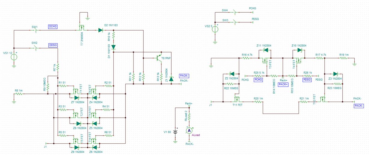
So far, I have created following schematic and need some help in verifying it:

I still need to calculate passive values.

Regards,

Anurag

  • Hi Anurag,

    Your other thread and the picture indicates you have a simulation in work.  TI has the TINA-TI and PSpice for  TI tools available. 

    In your circuit SW1 and SW2 should switch between 12V and GND to better simulate the function of a driver.  You might add the driver resistance if indicated in its data sheet.

    VS2 should be approximately 8.7 V less than V1 to simulate the function of the BQ76952.  If  you will be changing the voltage of V1 in simulation you may want to reference VS2 from the PACK+ voltage. Since the PCHG and PDSG signals are high impedance when off the SPST switches are appropriate at SW3 and SW4. 

  • Hi,

    Thanks for your response. I am using TINA-TI for simulation as my model isn't supported by Pspice.

    I will take a note of your points while simulating.

    VS2 should be approximately 8.7 V less than V1 to simulate the function of the BQ76952. If you will be changing the voltage of V1 in simulation you may want to reference VS2 from the PACK+ voltage.


    Does that mean, if my Pack Voltage is 60V then should I use approx 51.3V to simulate PCHG and PDSG.

    And can you tell me what is the advantage of low side or high side for a BMS?

    Regards,

    Anurag

  • Hi Anurag,

    Yes, for a GND referenced voltage for PCHG and PDSG on use 8.7V less than V1.  So for 60V use 51.3V.  Or connect an 8.7V source to provide a negative voltage from V1 so that the voltage moves with V1 should you ever change V1.

    Using high side vs low side is a choice in design.

    One choice might be from using whatever is directly supported by the ICs you use.

    A reason for high side switching is it allows simple GND referenced communication and signaling from the BMS.

    A reason for low side switching is that the control voltage for N-ch discharge FETs and the on voltage for charge FET is within the voltage range of the pack.  You can simply drive the gates as the diagram above and your schematic show.  It should be less complex to drive lots of low side FETs, but this may add complexity in communications with the battery requiring an isolated path.

    The system requirements for a product may require either high or low side switching which sets your choice, or may require isolated communication interface which would easily allow low side switching.

  • Hi,

    Thanks for the explanation.

    Is there any reference to calculate passive values for the above circuit? RDSG, RCHG, RGSPD, RBoff, Roff etc. from below image?

    And what is the use of PMOS FET, video states that it assists CHG FET gates to fall.

    But, how is it able to control anything if its gate is always connected to ground.

    As for following Schematic:

    I am getting This curve as Transient Response:

    Even though, all the switches are off, I am getting 46A consumption, Is there anything I am missing?

    Regards,

    Anurag

  • Hi Anurag,

    In general there is not a reference to calculate the components  RDSG, RCHG, RGSPD, RBoff, Roff.

    RDSG selected to provide an adequate turn off without being too fast.  You might calculate a turn off time with your total FET Ciss in the 10's of us.  Probably in the few kOhm range.

    RCHG might be similar to RDSG

    RGSPD select for how much current you want to allow quiescent, it will be a divider with RCHG to provide adequate gate voltage.   Might be 10's of kOhm to Mohm.

    RBoff might be similar or smaller to RGSPD, this adds to the DC load when on, pulls down the base when off, base current will be gained up by the PNP.

    Roff will be the resistance which turns off the charge FETs, with the limit of the current gain of the PNP. Probably 100+ ohms.

    Opinions will vary on component values, pick something which gives you the necessary performance.

    Simulations can be tricky, sometimes models have problems.  I would suggest adding probe points or additional meters to find the errant conditions, then find a fix. Perhaps it is an initial condition or a leakage in a model based on maximum possible temperature.  If you have a question on simulation you might post a question for TINA-TI.