This thread has been locked.

If you have a related question, please click the "Ask a related question" button in the top right corner. The newly created question will be automatically linked to this question.

LM5106: MOSFET drivers are dying for some mysterious reason

Part Number: LM5106

Hello,

We are using the LM5106 in our AHB for motor control. We are using F28379D to drive the enable and the signal pins of the driver. Because our control is complex (duty cycle limitations, the application is a SRM controller)) we cannot use a bootstrap driver, we are using 12V to 12V isolated power supplies for the high side driving. We still have a 0.47 uF ceramic cap between Hb and Hs. Our bus voltage nominally is 72V but can go upto 84V, when the battery pack is fully charged.

We were doing unit tests, that is when saw multiple failures of the driver chip.

In the unit test code, I disable the chips, set the input ports, after that I enable the two drivers in each phase. After the test that lasts a few mS, I disable both the chips. This is when they fail. The MOSFETs seem to be safe, atleast for now.

I know the question is a little vague, but the failures are real :-( Appreciate any pointers.

Thanks,

-Bhaktha

  • Hello Bhaktha,

    Thanks for your interest in our drivers.

    In order to accurately comment on the possible root cause of the issue, I'd like to review your application schematic around the gate driver to ensure that all the components are adequately sized including CVDD, Cboot (which from your initial thread seems a bit high).

    Also are the failures consistent on both phases of your system? Also if available, you may share waveforms around the driver during normal operations.

    Regards,

    -Mamadou

  • Mamadou,

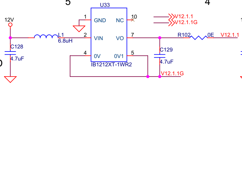
    Thanks for the quick reply. Here are the schematic snapshots, the driver and the isolated power supply.

    The "bootstrap" capacitor is 0.1 uF, sorry I said 0.47 uF.

    The failure is independent of the phases.

    The diode is DNP for now as we are not using the boot strap operation.

    The RDT resistor is now 100K, not sure if that matters at all.

    Our unit test is very simple, in the AHB of each phase I turn on the high side of the left arm and the low side of the right arm for 5 mS and make sure the current flows in the FETs and the motor winding. Very simple and stupid test and we are failing there.

    Thanks.

    -Bhaktha

  • Mamadou,

    While reviewing your response again, your comment on the CBOOT being too high raised a few alarms. The isolated power supply decoupling capacitor of 4.7 uF is now directly connected in parallel to CBOOT. Is that a big no-no ? Let me know. 

    Thanks,

    -Bhaktha

  • Hello Bhaktha,

    I am an apps engineer who works with Mamadou.

    I did not see the attachments of the schematics, but did see the component values mentioned. I assume the 4.7uF mentioned is capacitance on the isolated bias output and there is 0.1uF close to the driver IC. Can you confirm?

    It sounds like your operation where you have the issue, is when you turn on the high side FET on one winding terminal and the low side FET on the other winding terminal.

    I would suggest confirming the sequence of startup. I would confirm that the bias supplies to the driver IC are powered up and stable before applying inputs to the gate drivers or enable. This includes the VDD and floating high side bias. Confirm that the driver inputs are stable and low until the driver IC is enabled.

    If there is unstable bias, or unstable (indeterminant state) driver inputs when the IC is enabled that can lead to unexpected driver output states.

    Regards,

    Confirm if this addresses your questions, or you can post additional questions on this thread.

    Regards,

  • Richard,

    Re-attaching the schematic snapshots.

    Yes, the 4.7 uF is closer to the bias supply and the 0.1 uF is closer to the driver IC.

    Yes, the startup sequence you mentioned is what we are testing.

    Yes, the supplies are stable before we apply the inputs to the gate drivers and the enable signals.

    But .. you mention "Confirm that the driver inputs are stable and low until the driver IC is enabled." Can you please elaborate ? Is there a particular sequence of input to gate drivers and enable need to be followed ? Here is what we are doing. First we disable the driver, set the inputs and then enable the driver. Is that OK ? Or is there some other preferred combination ?

    Thanks.

    -Bhaktha

  • Sorry, schematics attached this time with a different method, I was copying and pasting directly from the schematic viewer to this window.

  • Hello Bhaktha,

    Thank you for attaching the schematics. Can you review the datasheet section 8 on sizing the boot capacitance, and confirm if the 100nF is adequate to drive the MOSFET Qg? I would make sure the capacitor close to the driver can drive the MOSFET gate charge.

    For the isolated bias, can you confirm the device used for the bias? Is the output fully isolated from the input with low parasitic capacitance on the bias output?

    For the startup timing, you might try enabling the drivers then setting the PWM inputs to the desired state.

    Can you provide scope plots of the driver input, LO and HO outputs, and enable during the startup sequence that is causing the issue.

    Confirm that all voltages on the driver pins are within the recommended operating ranges, VDD, HB-HS, IN, and HS to ground?

    Regards,