This thread has been locked.

If you have a related question, please click the "Ask a related question" button in the top right corner. The newly created question will be automatically linked to this question.

WEBENCH® Tools/TPS549B22: TPS549B22

Part Number: TPS549B22

Tool/software: WEBENCH® Design Tools

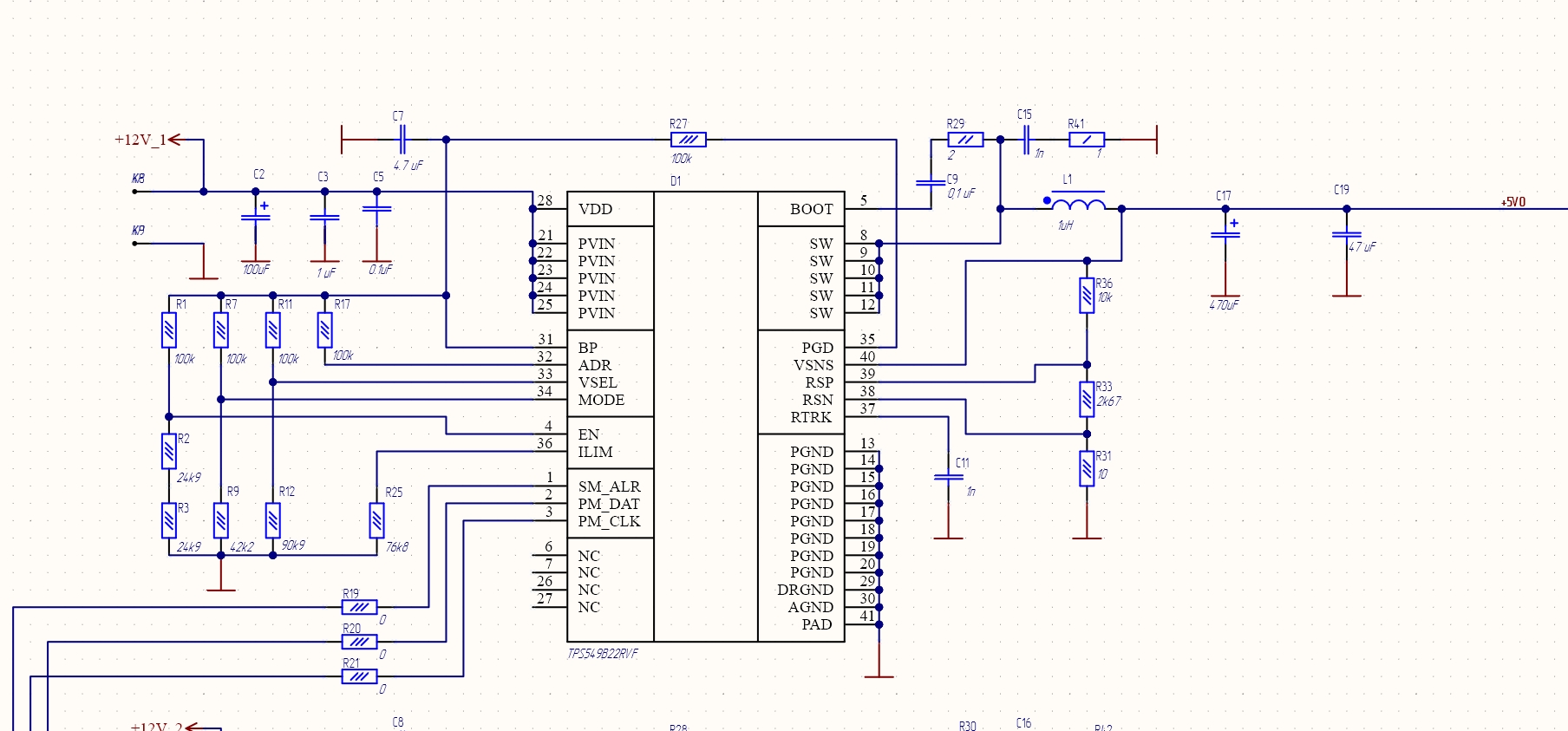
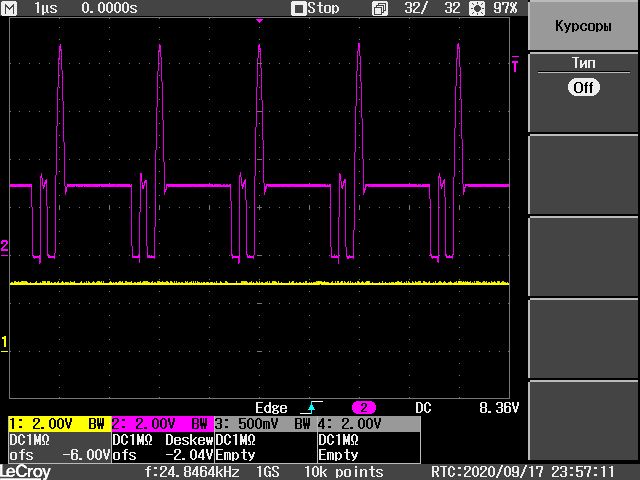
Hi. In my device, I have a problem with an output voltage of more than 3.3 V. for еxample, 5 volts. And in program Webench, too, it does not give 5 volts at the output, but only 3.5 V . Resistor Rrsp selected 0.001 mOhm . What is the problem? Thanks

  • Hi Gia,

    Can you share the schematic for your design and can you share a link to your WEBENCH design (or the WEBENCH design report)?

    Anthony

  • I found an error in the WEBENCH. It always sets the value of the resistor Rrsp=10 ohms.

    But my circuit does not give more than 3.5 V. (using PMBUS )

    Is it possible to make the output 5 volts, without pmbus (by default). With my scheme

    Tthanks

  • Hi

       Can you please share a link to the WEBENCH design?

    regards,

    Gerold

  • Design ID: 205
    Part Number: TPS549B22RVFR
    Design Name: TPS549B22RVFR 12V-12V to 5.00V @ 20A
    But I was already sort out with webench (I wrote it above). What's wrong with my schema?
  • Hi Gia,

    There is currently a bug in the WEBENCH schematic where Rrsp is being placed in the wrong location. The update is expected to show up on the web this week.

    I've taken a look at your schematic and couldn't find any obvious error. I have a few questions.

    1. Can you share the part number for C17?
    2. Are you adjusting any of the settings through PMBus, such as fsw and the ramp setting? For Vout > 2.5V, the R x 3 option is recommended. WEBENCH may also not be setting this value and I need to look into this closer.
    3. In the PCB layout, is the 1uF input cap placed across the VDD and DRGND pins? I don't think this would cause your particular issue but is something to try.

  • C17 -  T491X477M010AT  Kemet. We also tried to remove this capacitor, with only ceramics remainded. No difference.

    I've tried fsv=650 kHz and 1.125 MHz. With 1.125 MHz vout is about 0.2V higher than with 650 kHz.

    I've tried ramp select resistor x1 and x3 via pmbus (didn't use STORE_DEFAULT_ALL command), no difference. Can this resistor affect on output voltage?

    Do I need necessarily use STORE_DEFAULT_ALL command for some parameters, or all registers affect on work mode immediately, without power cycle?

    And also: Сhanged the parameters of the resistors in my circuit to R12=short  or open (Vsel=0.975V, NVM is unprogrammed, factory default), R33=2k43 . The result is the same

  • You may need to use STORE_DEFAULT_ALL for the RCSP setting and reset the device for the new setting to be used. It is not clear in the documentation I could find and I don't have a setup to test this myself today. I can get a setup tomorrow to help try as well if you are still having issues.

  • If we remove the resistors R33 (Rfbt), the output is only 3V.

    Is this normal?

    (We have 4 boards. And all behaves the same way)

  • Hi Gia,

    A couple other things I recommend checking if you have not already.

    1. Is input voltage 12V when you are testing this? It would be good to check with a DMM near the pins PVIN and PGND pins of the IC. The min off-time of 300ns would limit the maximum output voltage if the input voltage is low enough.
    2. Can you also check with an oscilloscope if the switching node is stable? Please measure with a timescale that shows around 5 switching cycles.

  • Another nuance.

    If we set  output voltage  3.3 V (via PMBUS, PVIN=VDD=12V) , the real output is 3.4V.

    But if the PVIN=VDD >15.5V , the chip gives an error
    Status VOUT:
    5 UVW Undervoltage warning
    4 UVF Undervoltage fault

    and turns off,

    datasheet: Input Voltage (PVIN): 1.5 V to 18 V

  • I tried to:

    1) set RCSP to Rx3,

    2) used STORE_DEFAUTL_ALL command

    3) reset the device (power on and off)

    This give no changes. The maximum output is still 3.5V, like there is some saturation.

  • Hi Gia,

    Thanks for the details from your testing. The behavior with the output set to 3.3V is also very unusual. I am waiting for a board to try this out myself to see if I can reproduce it or at least verify there isn't an issue with how you are setting the output voltage.

    In the meantime, can you help measure the SW node with an oscilloscope with a timescale that shows ~5 switching cycles to see what the device is doing when it is unable to bring the output up to 5V?

    Also, can you share some images of the PCB layout? If I find that I can get this to work on the EVM, this would suggest the issue is PCB layout related.

  • Thanks. I'm sending, Rload=22 ohmtps549b22.rar

  • Hi Gia,

    Something doesn't seem right with the SW pin waveform. It is only going up to ~3 V when it should be going up to VIN. Sometimes I see there are spikes up higher but this doesn't look normal. Assuming the voltage at PVIN is 12 V, it looks like the HS FET is not even turning on.

    Can you measure the BOOT pin voltage and PVIN pin voltage next? When the SW node is at ground the BOOT pin voltage should be near the BP voltage (near 5 V minus a diode drop). Insufficient BOOT pin voltage would prevent the HS FET from turning on normally but I don't see how this could be happening. I also want to make sure the PVIN voltage is sufficient when the TPS549B22 starts switching.

    One thing I noticed in the layout is there is not a dedicated bypass cap from VDD to DRGND as recommended. I wouldn't think this would cause the behavior we are seeing at the SW node but it could cause other issues.

  • Hi.

    New, more correct images

    1.jpg   - pin 5 (BOOT)

    2.ipg - pin 8...12 (SW)

    All is well on the VCC output. There are no drop

    2.

    The yellow beam is the output voltage

  • It definitely looks like the HS FET is not turning on at all and the BOOT voltage doesn't seem right either. When the SW node is low, the BOOT voltage is around 4.3V which is normal. When the SW node is at ~3V, the BOOT voltage should go up to ~7.3V but it is not. I wonder if there is an assembly issue from BOOT-SW. Please check to make sure the values are right and everything related to the BOOT-SW path is making a good connection to the PCB.

  • Thank you for your help and attention. I found a problem. Resistor Rbst was faulty

  • Hi Gia,

    Great! Glad we found the problem and you were able to fix it. Just let me know if you have any other issues.