This thread has been locked.

If you have a related question, please click the "Ask a related question" button in the top right corner. The newly created question will be automatically linked to this question.

TPS28225: Driver issues with pre-biased output

Part Number: TPS28225
Other Parts Discussed in Thread: CSD17556Q5B

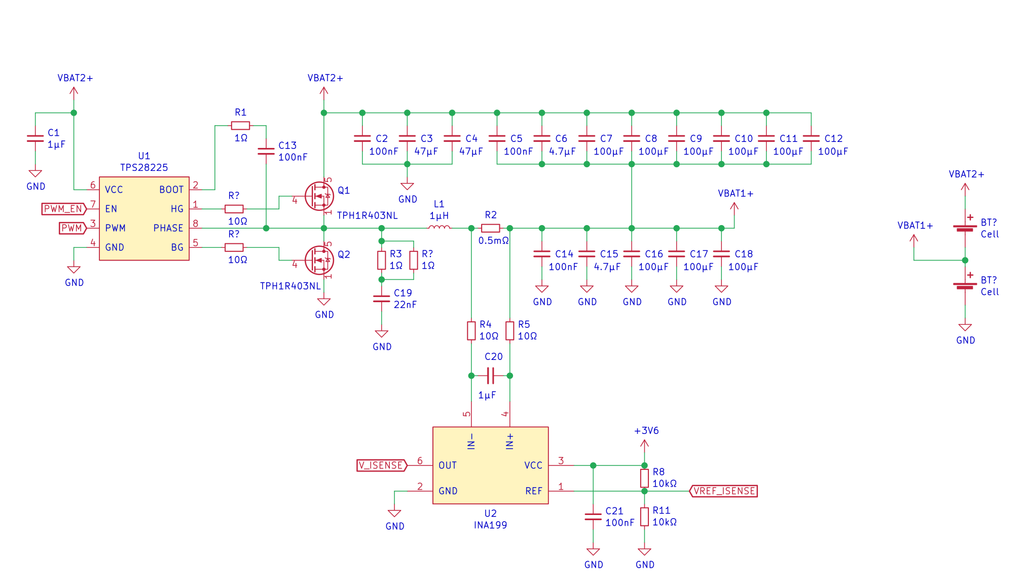
I am using the TPS28225 to drive two n-channel mosfets to balance two series lithium battery packs in a sort of buck-boost configuration. Here is the simplified schematic:
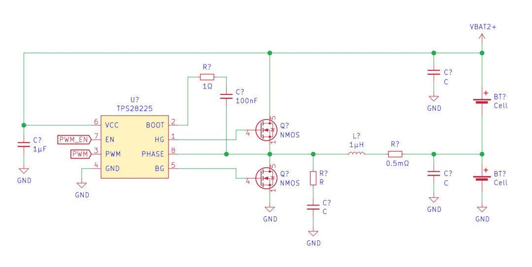
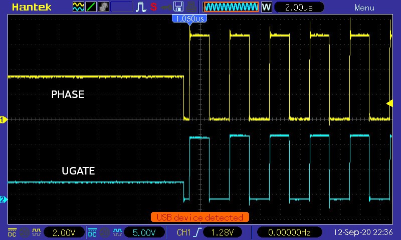
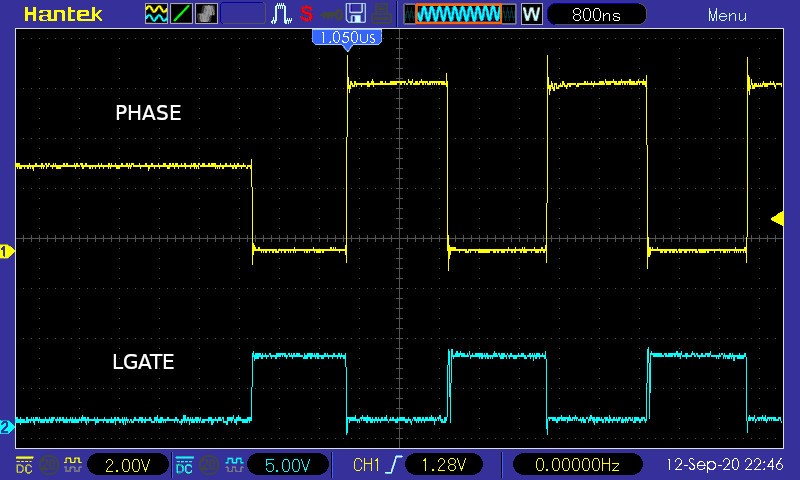
In testing the circuit at a 50% duty cycle the circuit worked as expected but as the duty cycle decreases and the current ramps up to around 5 amps the driver was outputting some bizarre waveforms and audible noise. The following waveforms were taken whilst the bottom cell was transferring current to the top cell (boost configuration). The duty cycles starts of at 50% and then decreases to about 35%.

Everything looks fine so far..

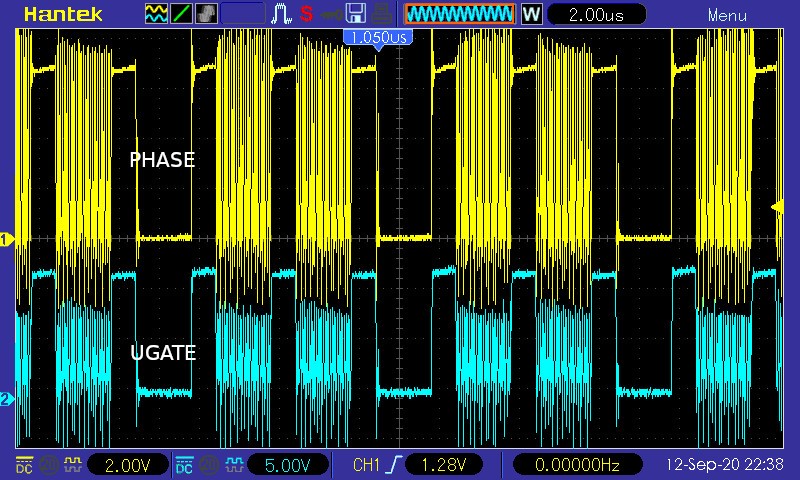
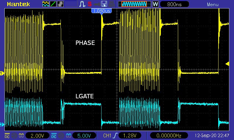
Then the gate driver start outputting some high frequency switching.

I checked to make sure the PWM input wasn't doing anything weird and it seemed fine, the EN/PG pin was also steady at 3V.

I initially thought that I had damaged the driver from switch node ringing so I swapped in a new driver and added an RC snubber with the same result. My new guess is it has something to do with having a pre-biased output.

Any suggestions would be greatly appreciated!

  • Hi, Jamie, That is odd, indeed. My colleague will be back in the office on Monday to work on this issue with you.
  • Hello Jamie,

    Thank you for the interest in the TPS28225.looking at the 3rd and 4 plots, I see that the Ugate is low amplitude when the HF switching starts, and that Lgate is switching also. The Lgate output should only go high when the PWM is low, but I see that the PWM signal seems clean but I do see a slight slope on the high (declining) and low (rising).

    Can you confirm if the PWM scope plot was measured close to the TPS28225 pins, with short connections and the plot is wide bandwidth? If not confirm the PWM waveform close to the IC pins. Although the plot seems clean the driver is behaving as if there is false triggering on the PWM input. You can try adding a small R/C filter on the PWM input with the cap placed very close to the PWM and GND pins. Try 50 Ohms and 47-68pF to start.

    I also see that there is a 1 Ohm resistor in series with the boot cap. It is possible the UGATE drive current is causing a drop in PHASE to BOOT voltage which may cause unexpected behavior in the UGATE output. Try shorting the resistor and make sure the BOOT to PHASE cap is placed close to the IC pins. Try taking a plot of the BOOT to PHASE voltage to confirm if this voltage is stable. Also the EN pin if there is noise could cause unexpected behavior, try adding capacitance to this pin.

    Confirm if this addresses your questions, or you can post additional questions on this thread.

    Regards,

  • Hello Richard,

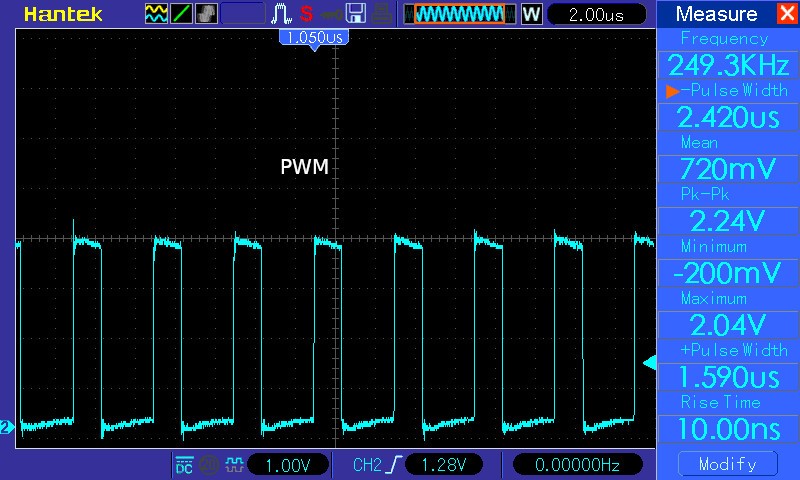
    Thank you for your response. I have shorted the 1 ohm resistor, added 100nF capacitor the the EN pin and added an RC filter to the PWM input. However unfortunately it had the same result as before. I even increased the the RC filter capacitor to 500pF. Under the scope the PWM pin now looks like this (measured using short connections at 100MHz bandwidth):

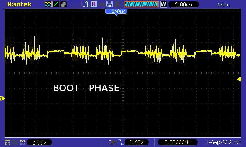
    Also here's what the waveform looks like between BOOT and PHASE:

    Do you have any other suggestions?

    Jamie

  • Hello Jamie,

    Thank you for the update. It looks like the PWM is clean so I don't expect that to be a concern. The BOOT-PHASE does show some ripple so it might be worth considering increasing the BOOT capacitance value.

    Can you provide the MOSFET part numbers that you are using? I would like to review the parts to see if there are concerns with body diode recovery time and gate charge.

    Can you try adding some gate resistance, to confirm if dV/dt may be creating some issues with either the driver or MOSFET device. Try adding from 2 Ohms and increase maybe up to 10 ohms just as an experiment.

    Regards,

  • The mosfets are TPH1R403NL. I will test adding some gate resistors. What seems odd to me is, if I remember correctly there were no issues at 50% duty cycle (when very little current was flowing). I also noticed in testing that if I didn't connect the terminal connecting the series batteries together to the unit and used it as a simple buck converter with no load there was no issue either.

    Jamie

  • Hello Jamie,

    Thank you for providing the FET part number. I did see one observation in reviewing the datasheet worth noting. There is not a parameter specified for the body diode recovery time which is an important consideration in sync buck or boost apps. It is hard to avoid conduction through the MOSFET body diode and once conducting it has to be forced off during the recovery time. This can lead to high dI/dt and dV/dt in the power train.

    TI has a similar parameter FET regarding RDSON and voltage rating with 36ns specified as the body diode recovery time. This part is also lower gate charge than the Toshiba FET.

    I would suggest trying this FET or another device paying attention to a fast recovery body diode spec. The CSD17556Q5B datasheet can be found here.

    https://www.ti.com/lit/ds/symlink/csd17556q5b.pdf?ts=1600195854918&ref_url=https%253A%252F%252Fwww.ti.com%252Fpower-management%252Fmosfets%252Fn-channel-transistors%252Fproducts.html%253Fpqs%253Dpaqs%2526familyid%253D1941

    Regards,

  • Hello Richard,

    Thank you for your help, after adding a gate resistor and and increasing the bootstrap capacitor the circuit worked as expected! I suspect it was the lack of gate resistor which was causing the problems. I think the boot phase ripple was caused by the extra switching.

    Jamie

  • Thanks for confirming this resolved the issue. You can post any new questions that you have.

    Regards,

  • Hello Richard,

    Using a 10 ohm resistor seemed to work, in boost configuration I had no issues, although using a resistor any lower than this caused the oscillations again. However when I tried it in buck configuration at startup it shorted the lower battery. I thought that this could be a prebias startup issue.

    So I tried a sort of soft start method using the TPS28225 diode emulation feature where I would only switch the high side mosfet at 50% duty cycle first, then slowly start switching the low side mosfet increasing its duty cycle up to 50% too. After this I would slowly adjust the duty cycle normally to the required value. This worked maybe 10 times in succession where I could get it to produce the full output current but the next attempt also ended up shorting the bottom battery at startup.

    Unfortunately I could not capture the waveform of the short. I also tried your other suggestion of using a different MOSFET with a better reverse recovery time which didn't help and also required a 10 ohm gate resistor to prevent oscillations. My guess is that possibly after the first 10 attempts the voltage differential between the batteries was greater and the soft start method didn't work so well. It seems to me that the short could be caused by the same oscillations from before. Maybe the 10 ohms gate resistors are not enough, however any more gate resistance and the MOSFETS start becoming too inefficient.

    Jamie

  • Hello Jamie,

    Thank you for the update. It is unfortunate to hear the issue came back with different operating modes and conditions. I have not mentioned or asked about layout details up to this point, but the layout of the power train high current loop and gate driver to MOSFET gate drive loop is an important consideration. If there are pwb trace lengths with high parasitic inductance this can cause high frequency ringing and voltage spikes in the power train and also the gate drive paths.

    Do you have pc board layout  that you can share? If the schematic you provided is not complete can you provide the complete schematic as well?

    Regards,

  • Hello Richard,

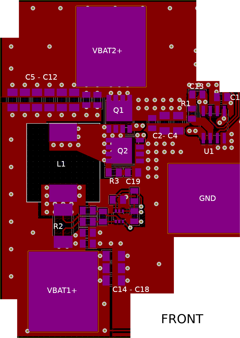
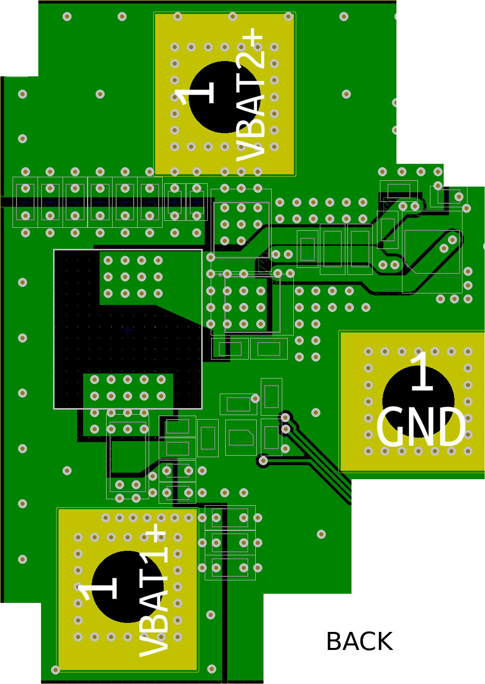
    I can only divulge the power section of the PCB and schematic, the gate resistors were not on the original design but were added on to the back of the PCB afterwards, but here it is:

  • Hello Jamie,

    Thank you for the schematic and partial board plots, the driver and power train helps. The VDD cap placement and Boot cap placement looks OK. There is a little distance from the driver to the FETs but does not seem excessive. I know you cant show the control section but not knowing where the PWM signal originates and EN signal I cant comment on those trace lengths or routing.

    The only things I can think that would cause the high frequency behavior would be relating to some high frequency noise or ground bound at the driver PWM to ground pins, or for some reason the FET's getting into a high frequency oscillation. I know that adding some gate resistance helped but did not resolve during all conditions.

    Can you try adding capacitance to the EN and PWM pins to confirm there is no ground bounce or noise issues at the driver IC pins. Try 68 to 100pF to start on the PWM pin. Enable should be able to have higher values if you are only using to enable and disable as an on/off function.

    Adding capacitance to the MOSFET gate to source directly on the gate and source pins can help reduce Vgs perturbations during the switching events. Try adding as an experiment 1nF directly on the gate and source pins of the MOSFETs.

    Confirm if this addresses your issues, or you can post additional questions on this thread.

    Regards,

  • Hello Richard,

    The PWM signal and EN pins originate just out of shot on the PCB layout I sent you. Also I have already tried adding some capacitance to those pins without success, I think you have previously suggested this. 

    I tried adding a 1nF capacitor directly between the gate and source of the MOSFETS this didn't change anything, I also tried increasing this to 3.2nF which didn't help either. 

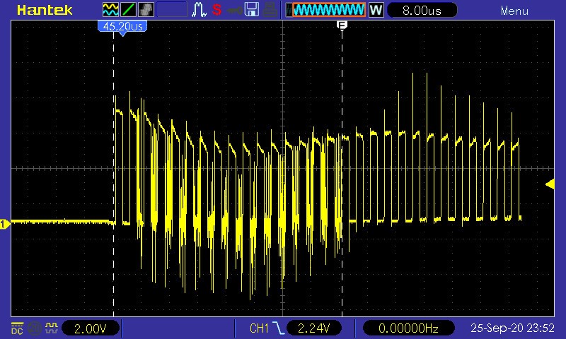
    One thing I have noticed is that ever since I have added gate resistors the high frequency oscillations only ever occur at startup previously these happened throughout. This follows with my previous testing - in that when it managed to startup in either buck or boost mode, everything worked perfectly even at 30+ amps. All the problems tend to be at the startup. These issues occur even when using the device as a simple buck converter (not having a battery connected to the output), also it occurs even when there is no load. 

    Here is the waveform of a startup as a buck converter with no load taken from the PHASE pin to GND:

    As you can see the high frequency oscillations only appear in the first 16 cycles or so.

    Jamie

  • Hello Jamie,

    It looks like the amplitude is changing during this startup process, I don't know if this is the phase node or one of the gate drive outputs.

    Is it possible the driver VDD is not stabilized on startup of seeing a transient which may cause what you are seeing.

    Confirm if maybe the driver VDD may need some additional capacitance to minimize the bias drop and recovery, or if this is the power stage Vin is it possible to increase that capacitance?

    Regards,