


Hi Guys,
Server PSU application and FB-LLC topology.
There will be a 42ns difference in the rising edge of MOSFET Vgs on the same bridge arm high side and low side. This 42ns will lead the real current 2A higher than set current.
If we use a linear DC source to supply power for the bootstrap drive of UCC21520, the difference in the rising edge of the MOSFET drive will be reduced to 14ns. Real current will be equal to set current.
So question:
What is the difference between the auxiliary power supply for bootstrap and the VDD bootstrap power supply? Why is the rising edge of the drive different? How to reduce the 42ns at VDD power for Cboot?
Eliminate the problem of power supply voltage, the auxiliary power supply and VDD bootstrap supply voltage are the same. Also keep the input pulse width INA=INB;
|
VDD power for Cboot |
Additional DC source power for Cboot |
|
|
|
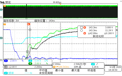
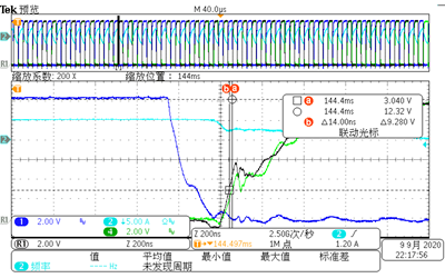
CH1:high side output; CH4:low side output; Black(For reference): high side turn-on, falling edge in phase with low side; CH2:FB-LLC primary current;
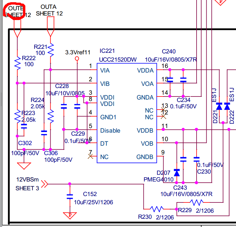
Please find the UCC21520 schematic. Meanwhile, we also tested the Cboot waveform by using differential probe. Seems normal. Please find the attachment.
Thanks
-Pengfei
