This thread has been locked.

If you have a related question, please click the "Ask a related question" button in the top right corner. The newly created question will be automatically linked to this question.

UCC256402: HHC Control technique

Part Number: UCC256402

Hi,

I am using UCC256402 for half bridge LLC converter,

specs are below:

Vin : 80V

Vout : 300V, 2amp

issue: I have set output voltage 300V and I am getting the same with no load condition but when I connect 2amp load, output voltage decrease to 294V and due to this voltage at feedback pin goes in to saturation i.e. 7V.

What could be the reason for restriction of output voltage at 294V when it subjected to 2amp load ?

I am using UCC25640x design calculator tool for component value calculation.

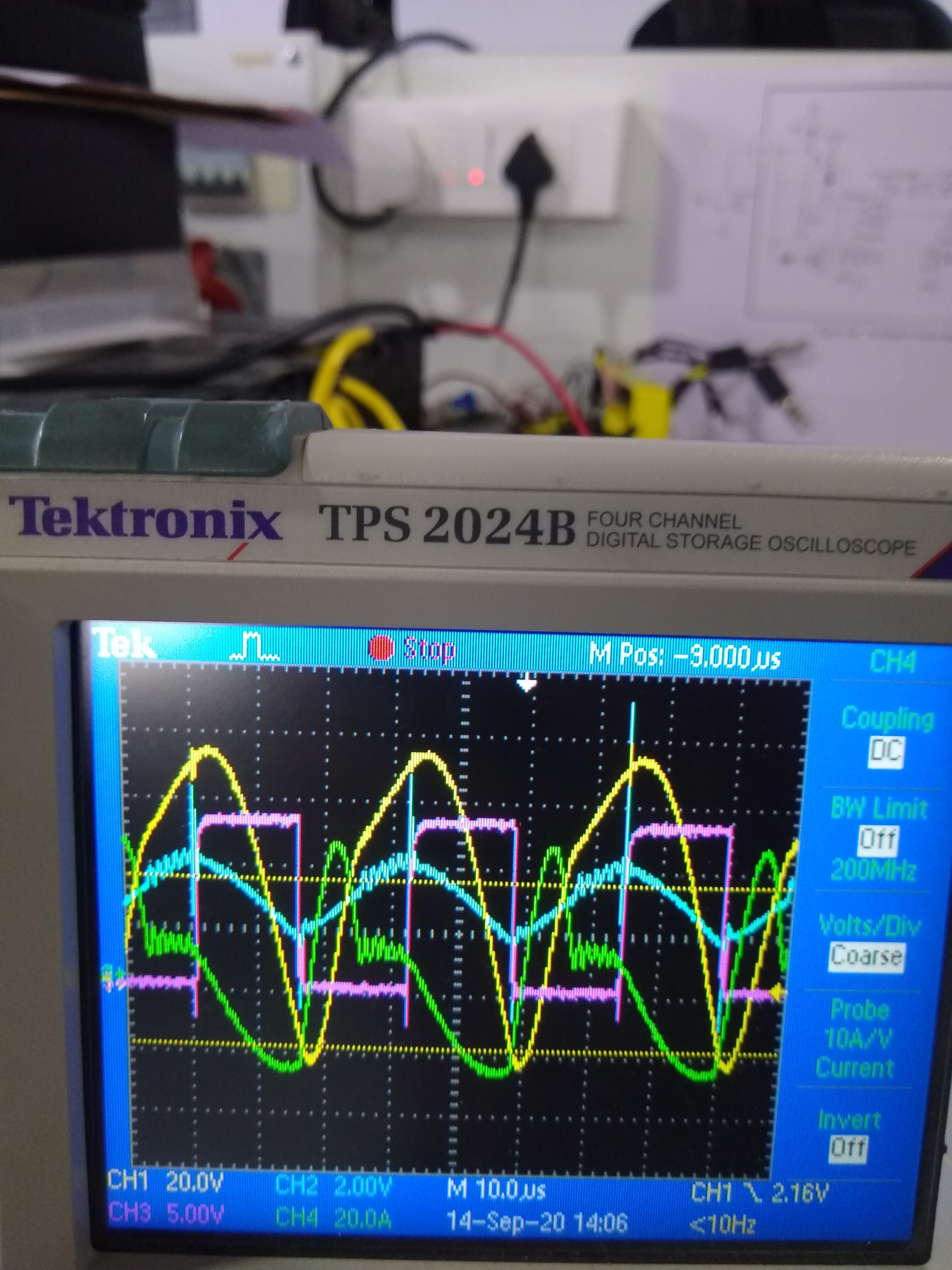
I have attached waveform image where yellow signal is low side mosfet's gate, blue is high side and pink is Vcr.

Vcr waveform is not symmetric to Vcm !!!  what is the reason for this ?

Which control technique is applying here (charge control method or Direct frequency control ) ? 

How to know whether the frequency compensation ramp is dominating or resonant capacitor voltage is dominating ?

Thanks,

Jitendra

  • Hi Jitendra,

    The VCR pin max control range is 6V to 0V. The controller will not push the VTH and VTL threshold above or below this range. Once the range is maxed out, it acts as a "min frequency clamp" so this is why you are seeing some droop in the output voltage at heavy load.

    There appears to be a large amount of noise coupling into VCR whenever one of the gates turns on and is causing a large discontinuity in the VCR waveform. I would suggest taking a look at the layout to see what is causing the large amount of noise coupling into VCR here.

    This controller uses charge control with a frequency compensation ramp on top. Based on the VCR waveform, it seems both have a relatively equal contribution to the total VCR waveform.

    If the frequency compensation ramp dominates the VCR waveform, the VCR waveform will look like a triangle wave. If the resonant capacitor sampling dominates the VCR waveform, the VCR waveform will look sinusoidal, following the resonant capacitor peak to peak voltage.

    Best Regards,

    Ben Lough

  • Hi Ben Lough,

    Thanks for reply,

    There is some noise observed in this waveform but by changing Vcr divider capacitors, I also get smooth waveform ( see attached image) so I think there is no issue of pcb layout.

    Here,

    Pink: Low side mosfet gate waveform,

    blue: Vcr

    yellow: Resonant capacitor voltage waveform

    green: Resonant capacitor current waveform (captured by current probe)

    these waveform look better than before but still output voltage is restricted at 294V with load.

    Resonant capacitor current waveform doesn't look in proper sin shape, what could be the reason for this ?

    I have tried to change Vcr capacitor ratio a little bit, I observed changes in amplitude of Vcr signal's peak and valley points but there is no change observed in frequency and duty cycle.

    What should I do to enter in charge control scheme ?

    My resonant capacitor value is 2uF,

    Vcr cap_lower : 20nF ( This is not exact value of what "UCC25640x design calculator tool" calculated, I tried with tool's calculated value but no benefit found)

    Vcr cap_upper: 500pF

    How much change ( increase or decrease ?) I should do in Vcr capacitors to trigger charge control scheme ?

  • Hi Jitendra,

    The resonant capacitor voltage shape is following the resonant current. Notice the change in slope occurs as the resonant current amplitude changes. The resonant current shape suggests the LLC is operating very far below resonance. 

    I would suggest checking the reference point on the FB divider. Perhaps there is some voltage drop causing the regulation point to be off as the load increases. Also do you still see the FB pin voltage go up to 7V and the VCR pin peak to peak >=6V with load?

    Best Regards,

    Ben Lough

  • Hi Jitendra,

    Also I would suggest checking the inductance of your secondary side windings. It looks like when the high side is on, the converter is operating below resonance and when the low side is on, the converter is operating above resonance. The VCR waveform seems to be reasonably centered on 3V in the scope capture you shared so the waveform suggests the secondary windings are not well matched in their inductance.

    Best Regards,

    Ben Lough

  • Hi Ben,

    Waveform attached in my previous reply is generated with following LLC configuration,

    Inductor: 3uH,

    transformer (primary) : 15uH and

    Resonant capacitor: 3uF

    I have checked reference point on FB divider which is stable (not changing with load), and yes, voltage at fb pin is 7V, Pk-Pk Voltage at Vcr is not > 6V as you can see in previous reply.

    Regards,

    Jitendra

  • Inductance of secondary side windings are 300uH and 302uH i.e. both are identical.

    So this is not the reason for non symmetric Vcr waveform !!!

  • Hi Jitendra,

    Thanks for the additional info. Please share your schematic. I will review.

    Best Regards,

    Ben Lough

  • Hi Ben,

    Can you share your email ID where I can send schematic?  I can't share it publicly.

  • Hi Jitendra,

    I direct messaged you. You can direct message me the schematic.

    Best Regards,

    Ben Lough