This thread has been locked.

If you have a related question, please click the "Ask a related question" button in the top right corner. The newly created question will be automatically linked to this question.

LM5051: Inquiries about the operation of the LM5051

Part Number: LM5051
Other Parts Discussed in Thread: LM5064, LM5069, LM5066I, LM5068

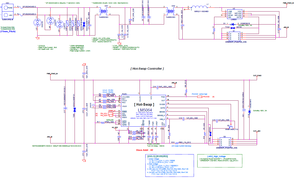
When configured with the attached circuit, as a result, -48V output does not occur between PWR_PGND_IN and -48V_IN.
PWR_SW is in OPEN state.
When measuring the voltage for each section, it seems that the FET of Q1 does not work because there is no VCC output voltage of LM5051.
I do not know which part of the circuit has a problem, so I contact you.

  • Hi Park,

    Apologies for the delay. This thread got missed due to change in the role and responsibilities of our internal team members.

    What is the applied voltage between LINE and VSS ? What is the voltage you observed between VCC and VSS ?

    Does the VCC came up when you replace U2 with fresh unit ?

    Best Regards, Rakesh

  • It seems that the problem was that 48V was applied to PWR_SW. After changing to a new IC, it was tested in the open state and it worked normally.
    I would like to inquire further.
    I want to implement a power switch in a circuit that only has 48V. What should I do? Should we implement power On/Off on the LM5064 side? I share an additional schematic at the back of the circuit above. I want to implement it with switch open/drain.

  • Hi Park,

    For +48V rail ON/OFF control, look at LM5069 or LM5066i

    For -ve rail, please see LM5068, LM5064

  • I have further inquiries from LM5051. Even if the LM5051 is removed from the top schematic, the output is -48V. Isn't Q1's FET Drain and Source connected in reverse? It was constructed by referring to the datasheet.
    During the test to implement power on/off, I tried to open the LINE pin of LM5051, but it is output to PGND_IN and -48V_IN.
    So, I tried removing LM5051 at all, but it still prints.
    I suspected a defective FET, but it was confirmed that the drain and source are open, but the output is nevertheless to PGND_IN and -48V_IN.
    I would like to know if there is a problem with the FET characteristics or the circuit configuration.

  • The body diode of the external ORing MOSFET provides the path. Can you load 1A at output and measure voltage drop across the MOSFET.

    Best Regards, Rakesh

  • It's my first time designing a power supply, so I don't know a lot.
    In particular, there are many areas where the operation of the LM5051 is not understood.
    The ORing function doesn't seem to work.
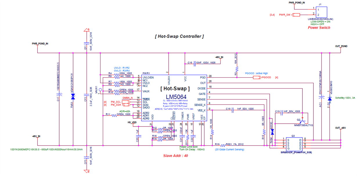
    The circuit diagram below is the Unit (Power Supply Unit).
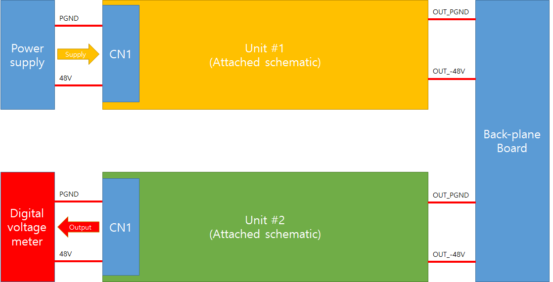
    When Unit #1 and #2 are connected to the backplane and power is supplied to #1 as shown in the configuration below, I think it should not affect Unit #2 by LM5051 (not supplied to Unit #2).
    By the way, when power is measured in Unit #2, -48V is output.
    I don't know why. Doesn't it make sense to use the LM5051, or is there a circuit problem?
    Should the LM5051 be configured after LM5064 (OUT_PGND side)?
    Even if the current circuit has an effect on the LM5064, it doesn't make sense that the power is output to CN1.

    Thank you for your help and want a little more help. thanks.

  • Further experiments were conducted.
    After removing TVS2 and TVS3, measuring at UNIT#2 with the same configuration as above, about 4V is output. It seems that the LM5051 cannot block all of them. How to cut off with 0V?

  • Hi Park,

    Reverse current flow is needed to turn-off the ORing FET. To confirm this as the root cause, please use diode in place of Q1 and check once whether you still see voltage at unit#2.

    Best Regards, Rakesh

  • Hi Park,

    Do you have any follow-up questions. ?

    Best Regards, Rakesh

  • Many questions seem to have been solved. No questions regarding the LM5051. Thank you, Rakesh.

  • Thanks,

    Best Regards, Rakesh