This thread has been locked.

If you have a related question, please click the "Ask a related question" button in the top right corner. The newly created question will be automatically linked to this question.

UCC27714: Low-side MOSFETs disabled but getting hot, with 5% high-side PWM.

Part Number: UCC27714
Other Parts Discussed in Thread: TPS2024, , CSD18537NKCS

Hi,

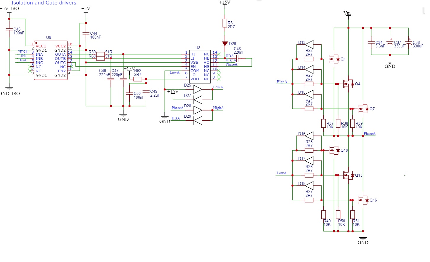
I have the circuit shown in the attached schematic. It shows one of the three motor phase drivers that wil be used to drive a brushless D.C. motor. I am currently using an external D.C. power supply set to 40V and a current limit of approximately 4A.
https://e2e.ti.com/cfs-file/__key/communityserver-discussions-components-files/196/High-side-fets-not-working.jpg

MOSFETs are FDP61N20

U9 is isolation ISO7730FDWR

U8 is the UCC27714

D26 is standard diode VS-3EMU06-M3/5AT

Other diodes are shottky DSS120UTR

Note that the R22 through R27 have been changed to 100R.

The problem I am getting is that the low-side 3 MOSFETs are all getting hot when the bridge is operated with a high-side drive of 5% PWM and the low-side is disabled. I am using a single channel of a BLDC motor as a load connected between the bridge output and GND, so not currently using the low-side drive for this test. This causes the current shown on the D.C. power supply to increase by about 250mA.

I have tried connecting the gate and source for each of the low-side MOSFET's to ensure that they cannot be being switched on, but still they are getting hot.

I do not have a differential scope probe but can use two channels of a scope (TPS2024) to effect the same thing using difference measurements if this would be of help.

Regards

FarmerJo

  • Hello Farmer Jo,

    Thank you for the  interest in the UCC27714 half bridge driver. It sounds like a thermal and power dissipation concern when the low side MOSFETs are operating with the current conducting in the body diode. Depending on the operating conditions, mainly average current in this condition, and/or if the current is always positive (CCM), there may be concerns with the power dissipation from the average current thru the body diode drop, Vf x Iavg, or there could be switching loss concerns from forcing off the MOSFET body diode conduction.

    The experiment you performed, shorting the low side FET's Vgs does address a possible concern of the low side FET's turning on due to miller charge coupling into the gate.

    I see the FET's you are using has a body diode recovery time of ~140ns. Can you see if there are similar FET's you can try with faster body diode recovery? If you do not need the 200V rating usually  lower rated Vds MOSFETs can have faster body diode recovery times.

    Increasing the gate resistance that you indicated, is another suggestion I would have made to reduce the reverse current from body diode conduction.

    Can you confirm the operating current conditions in this operating mode? How high is the average current, and is the current always positive (CCM)?

    Regards,

  • Hi Richard,

    Many thanks for the help.

    I have since tried another MOSFET type with a much faster body diode recovery time of 50nS (CSD18537NKCS) but unfortunately the heating problem has persisted. This is with the gate and source connected as before. I have taken scope readings of the gate/source and drain signals and can see that in our design the drain signal overshoots on the rising edge to about 50V and undershoots on the falling edge to about -4 or -5V when using a power supply of 30V. It looks as though it is the undershoot that is causing the heating problem.

    The motor winding current is about 150mA measured using a current clamp. It does not appear that the motor current goes negative.

    Regards

    FarmerJo

  • Correction, the average motor current is approximately 150mA as shown on the external PSU and the peak motor current is about 1.5A indicated by the current clamp.

    Regards

    FarmerJo

  • Hello Farmer Jo,

    It does not sound like the average current of 150mA through the body diode, even if constantly conducted would explain any thermal issue. Also changing to 36ns body diode recovery should have made some difference I would have expected if there was a diode recovery/switching loss issue.

    Right now it is not making sense why the low side FET's would get hot in this condition, and not be an issue (I assume) at higher load conditions.

    Can you confirm if this is the only operating mode that you see the thermal issue?

    Can you provide scope plots in this operating condition of the following in this operating mode: HI, HO-HS (differential if possible), HS, current from switch node into load. Take several cycles and zoom in one one cycle to see the turn on and turn off details.

    If you can start and run the unit in this load condition, for a test case I would suggest confirming one more experiment. Can you remove the low side FET's and replace with ultra fast recovery diode(s) or schottky diodes to see if the diodes have high thermal rise in this condition?

    Regards,

  • Hi Richard,

    Thanks for the help and advice. This is what I have found so far.

    The problem appears to be solved when instead of connecting the phase output (Phase A) through the load and to GND, it is instead connected to a different phase where the low-side is enabled (and the high-side is disabled). The hardware has three channels in total. Don't understand why this would be but the low-side devices no longer suffer with the heat problem! Any ideas on this?

    There is another, possibly related issue, where we are destroying UCC27714 devices on a regular basis.The failure mode is that the HO output just stops working and no longer drives the high-side MOSFETs. Under this failure the device EN is high (enabled), LI is low and HI has a 10% PWM signal. I am wondering about the requirements for the 15V supply that we are using to power the UCC27714 and how stable it needs to be. Currently the 15V is being generated using a step-down regulator (MP9488). Is it possible that a problem with this supply could damage the UCC27714 devices?

    Will also get some scope traces this weekend as suggested and will add them shorty.

    Regards

    FarmerJo

  • Thanks FarmerJo,

    Richard will be back on Monday and I agree let's start with scope shorts. you could trigger during start up and other scenarios. Richard mentioned switch node current into load will be good one to see any abnormal conditions.

    Good luck and look forward to your waveform.

    Wei

  • Hi,

    Appologies for the slow reply.

    I have now fixed the stability issues with our 15V supply used by the UCC27714 device.

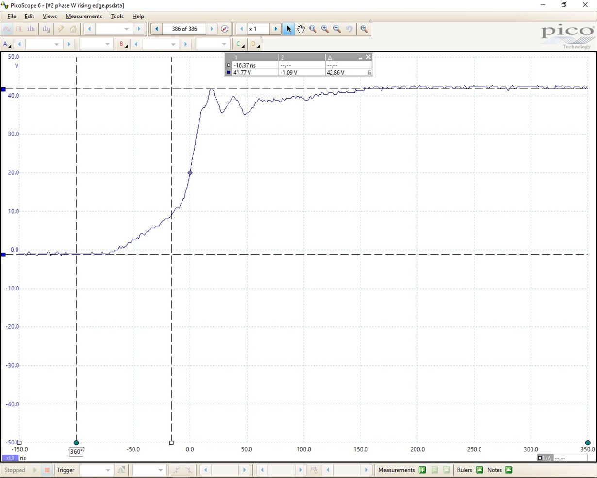
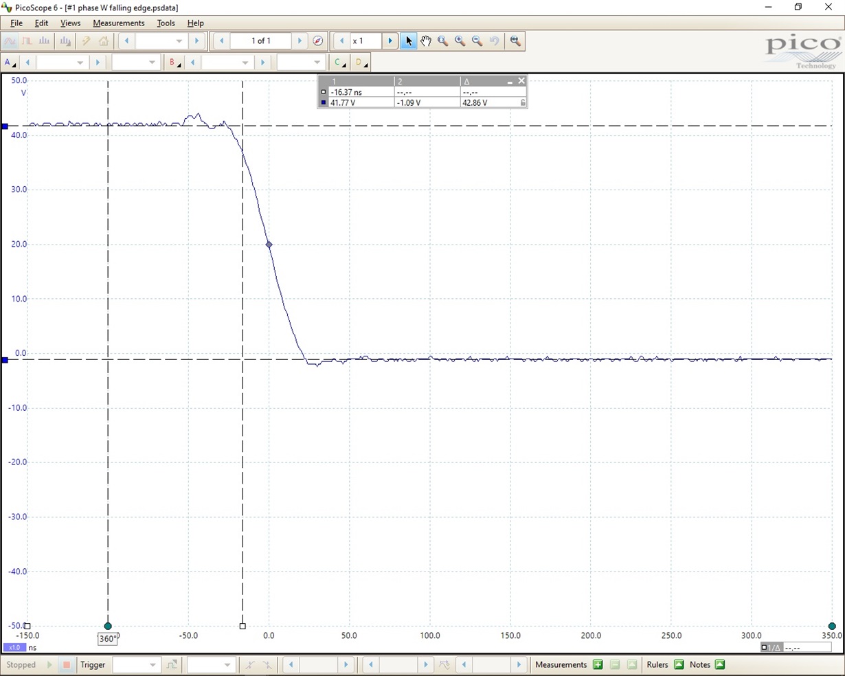
    I have attached a number of scope traces of phase W bridge output in addition to some VDS measurements across the MOSFT that is disabled but still get hot.

    The first two waveforms are of the phase W output. We are using a 30Khz PWM frequencey with an on time of about 10%.

    How is it that the upper voltage driven from the bridge is higher than that of our supply voltage of 40V?

    Also I notice that waveform 2 shows that the low-level driven voltage is about -1V where I would have expected it to be 0V!

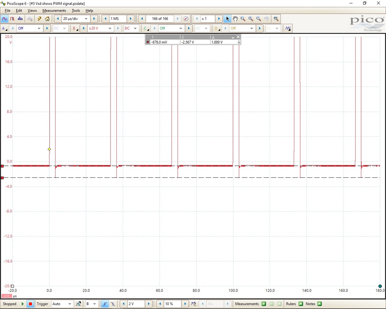
    The remaining 4 waveforms were taken using a x1 probe and show the voltage between the source (GND) and the drain of Q12 (see previous schematic).

    From these it appears that the drain pin of Q12 is driven negatively for a very short period in each PWM cycle.

    Is there any explaination why we are seeing a -ve drain voltage under these circumstances?

    Since attaching the original schematic I have changed all the 2R7 gate drive resistors with 100R values.

    I have not included any gate drive waveforms because previously I connected Q12 source and gate together and still the device gets hot. If it would help I can include these.

    Regards

    FarmerJo

  • Hi,

    Appologies, I am having difficulties in attaching the last waveforms, will try again shorly.

    Regards

    FarmerJo

  • Hello,

    Thank you for the recent scope plots. On the 1st plot and the question on why the switch node might go higher that the input source voltage. There is a current path from the high side drive which is higher than VIN of 40V, that sources current into the gate to source during the Vgs rise time. That gate drive current flows into the gate to source capacitance which means there is gate drive current flowing out of the MOSFET source. Normally there is a low impedance on the MOSFET source and you don't see much of an impact, but in theory this could cause the source to rise. Also depending on the current polarity there could be current flowing that may cause the body diode to conduct which would raise the source over the drain voltage.

    In the plot showing the slight negative voltage, this could be due to the body diode conduction if the low side MOSFET is not turned on.

    I think you mentioned one of the FETs is disabled which I assume is the low side FET. this would explain the ~-1V since the low side FET body diode can conduct.

    The narrow negative spikes are commonly seen to some degree and is cause by the dI/dt during swithing off of the high side FET which causes a voltage potential across the power train parasitic trace inductance. This can lead to short duration negative spikes.

    Confirm if this addresses your questions.

    Regards,

  • Hello,

    You can post the additional information when you have the plots available

    Regards,

  • Hi Richard, I cannot seem to add the remaining 3 waveforms. I am getting reports that my new posts are duplicates, although I am not able to see the new plots on the forum. Can you see them? Can they be attached in another way? I have been taking screen grabs so far and dropping then into the post. Worked for the first 3 but not the rest.

    Will try again soon.

    In the meantime, another thought has come to mind.

    If due to some timing issue both the high-side PWM signal was enabled and the low-side (non-PWM) was enabled at the same time for a very short time, would it be possible to cause damage to the UCC27714 devices. Another possibility of incorrect timing would be where two high-side (PWM) signals were driven into the remaining third enabled low-side driver. I can see that this would not do the MOSFETs a lot of good but is ther a mechanism by which the UCC27714 could be destroyed?

    Regards

    FarmerJo

  • Hello Farmer Jo1,

    I saw a notification of a post come in but do not see any latest activity. Just checking to see if you are having issues with the forum.

    Regards,

  • Hi Richard,

    Since we last spoke I have made two major changes to our drive as follows:

    There was a problem with our 15V supply to the UCC27714 where it was actually operating at about 12V with poor regulation. This has since been resolved.

    I have rewritten the driver firmware using C replacing the original FlowCode code. With the FlowCode code there was occasional bridge timing issues where at high speed there was an occasional judder in the motor output which was incorrect drive for two consecutive sensor transitions. Perhaps there was a bridge short here. Using the new firmware there is no judder at all across the entire speed range (up to about 12K RPM). Also there has been no damage to the UCC27714 devices either.

    Is there a failure mode that when the bridge high-side and low-side drive is enabled at the same time, even for short time periods in the mS region, that it could somehow cause the UCC27714 devices to become damaged?

    There is also another oddity in our 15V supply, in that when we power-down the controller (i.e. switch off the external voltage supply) and it falls below about 10V, it looks as though it tries to restart a number of times before the supply voltage finally dies. It swings between about 10V to GND at a frequencey of a couple Hz. On the first GND the processor should have reset and all the controll signals to the UCC27714 should be disabled. During this time the bridge will be powered at about 10V and the 15V input will be swinging between 10V and GND a couple of times.

    Does it seem feasable that this could cause damage to the UCC27714 devices?

    Regards

    FarmerJo

  • Hello FarmerJo,

    Richard is out of office until Tuesday meanwhile I may comment based on your latest questions.

    I have reviewed the driver IC schematic and I can confirm that the IC can support both HO and LO being HI so long as the bias supply is not in UVLO conditions (9.1V on, 8.6V off) AND that you application does not have potential shoot-through conditions on high-side and low-side gates.

    Based on your feedback, it sounds like your 15V supply might not be stable enough during this period and it is possible that the IC fails when the control signals are not disabled AND the supply is swinging 10V and 15V which goes against the recommended power sequencing of the IC (the IC should only see IN signal when the supply is stable and beyond UVLO to prevent potentially biasing ESD cells and allowing the driver internal circuitry to be biased before PWM signal).

    Please confirm if this addresses your inquiry or let us know if additional questions.

    Regards,

    -Mamadou


  • Hi,

    Having looked further into the problem of damaging the UCC27714 devices it appears to happen under two circumstances that both cause high bridge current and the external PSU to current limit.

    (*) Driving the motor hard.

    (*) Setting the external PSU current limit too low.

    I have since used slower ramp up times and have set the external current limit to 15A both of which prevent the sudden loss of the bridge supply voltage.

    My questions are now as follows.

    Would the sudden loss of the bridge supply voltage and corresponding loss of the UCC27715 15V supply cause damage to the UCC27714 devices if the bridge was driving motor phases at the time?

    Is it possible that somehow during very high bridge currents (probably higher than the MOSFET rating of 50A for a short while) that an incompatible voltage could be back driven into the UCC727714 high-side output pin destroying the device?

    Is there a method of protecting the UCC27714 devices under these supply voltage conditions? Is it quite possible that the external power supply could fail when motor is in operation, for example.

    Any help would be appreciated.

    Regards

    FarmerJo

  • Hello Farmer Jo,

    It is good to hear your latest changes have, I assume, resolved your remaining issues. The questions you asked regarding loss, or drop of the bridge input voltage and same with the driver bias, in itself would not damage the driver IC.

    However, most importantly if the driver bias was unstable and dropped to the point of being below the gate driver UVLO this would cause totally unexpected switching cycles in the bridge which could lead to the driver being exposed to voltage(s) on the driver pins that could stress the driver. If the driver stopped and/or started unexpectedly while the power train is conducting high current there could be voltage spikes much higher than normal operation.

    I would confirm that the driver VDD maintains a level of 10V which is the recommended minimum for this driver under various transient conditions.

    Confirm if this addresses your questions, or you can post another question on this thread.

    Regards,