Other Parts Discussed in Thread: TPS65130
Hi everyone,
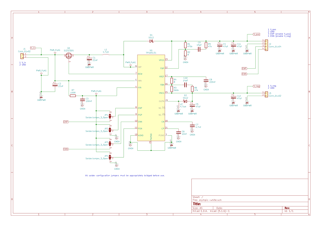
I've designed a small DC/DC module implementing the TPS65131 chip. The goal is for example to provide dual voltage (let's say +/- 12V) from a single 5V USB port supply.
This an "open source" project and I intend to put everything (Kicad files) on github. I'm basically a software engineer and hence a noob for hardware so I would welcome some comments and suggestions from you experts ! :)
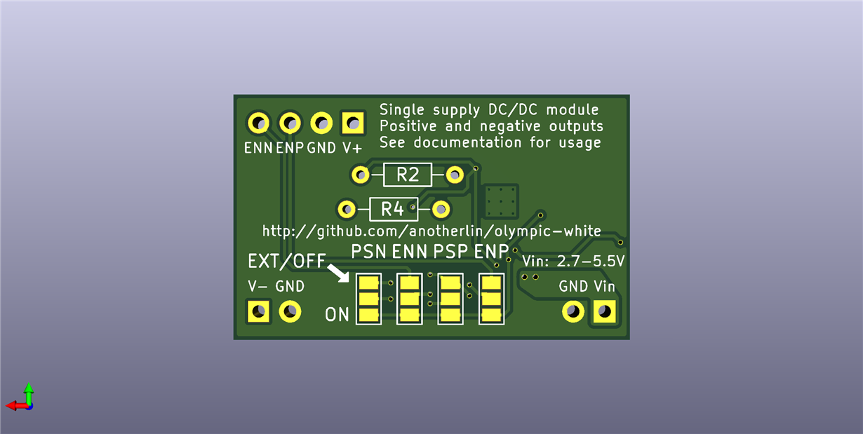
Please have a look at the schematic. The idea is to have a "programmable" module, that is we can select the output voltage using resistors (R2 and R4). I've also added solder jumpers so power saving mode can be enabled or not. And the enable signals can be always on or controlled by externally. R2, R4 and the solder jumpers are bottom side.
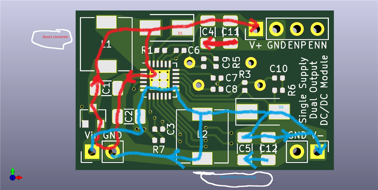
My main concern is regarding layout, which is something important for DC/DC converters. So I've taken great care to have big traces on top for both the boost and inverting (buck-boost) converters. In particular, GND is routed top sided as well as being "back plane" on bottom side. For supply, there is only one (double) vias for V- input. GNDA is routed on the bottom towards a "star" connection at the TPS65130 pins. The only mixed top/bottom signals, are the control signals (ENP, PSP, PSN, ENN).
Any obvious mistakes I've made?
Thanks for your help! :)
Best regards,


