This thread has been locked.

If you have a related question, please click the "Ask a related question" button in the top right corner. The newly created question will be automatically linked to this question.

LM5145: Over-/undershoot, offset low side FET

Part Number: LM5145
Other Parts Discussed in Thread: LM5146-Q1

Hi

I'm using the LM5145 with two CSD19532 for my DCDC stage. I have two issues.

First

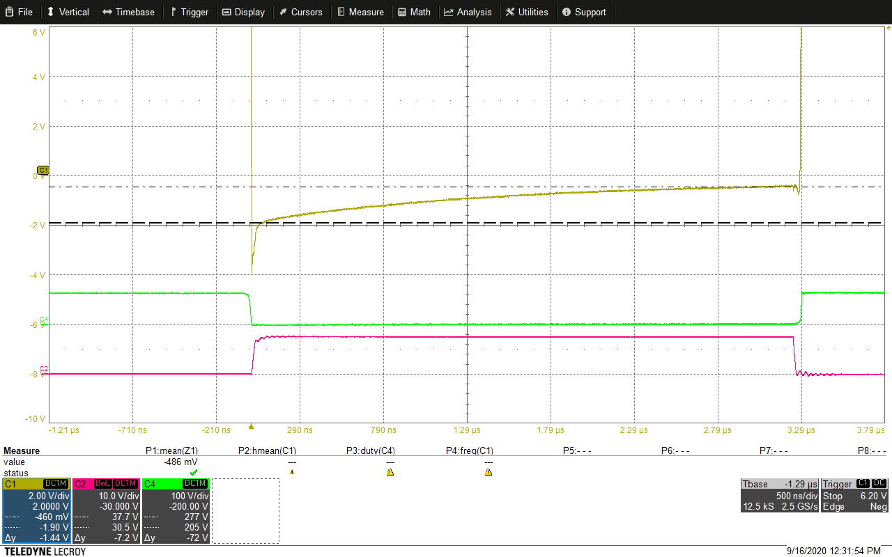
I have an over-/undershoot that I could reduce but it looks like that the solution (increasing gate resistors up to 33Ohm) is not the best way to solve it. Do you have an advice?

Second

When the low side FET is on, the negative voltage over the low side FET is larger as expected. Can you explain that?

Please check the attached word file. I have added all information into this document.

BR

SilvanoDCDC_Stage_Issue.docx

  • Hello Silvano,

    Gate resistor would be the ideal solution, as we cannot control the gate drive strenth by other means. You can reduce ring by snubber or boot resistor, corresponding to high-side turn-on, though those too will result in loss.

    For turning on high side vs low side, potential to have appropriate VGS for conduction is needed. Source for low side is sitting at GND. Source for high side is sitting at Vout, thus absolute voltage of high side gate voltage will be higher.

  • Hi Marshall

    Thanks for the fast answer. 

    I think the first question is ok for me.

    Concerning the second question:

    I have checked the Vgs voltage and I also have increased it up to 12V. Please check the plot below. From my point of view, the low side FET should be 100% on. I can't understand why the voltage drop is so high when the current is around 8A.

    The point is not only the power dissipation. It is also that the SW pin of the LM5145 should not be below -1V longer than 20ns. So it looks like that the signal below could damage the IC.

    Thanks for the help.

    BR

    Silvano

  • Hello,

    The SW pin should go no less than a diode drop below ground.

    Are the external MOSFETs appropriately connected?

    Are the external MOSFETs appropriate for this application? What is the part numbers? Are they NMOS?

  • Hi 

    The SW pin is the main reason why I'm asking.

    Yes I'm using nmos and they are very well connected. Please check the attached word file with the schematic and the layout.

    Concerning the part that I use. I'm using the CSD19532. I think it is a good choise, but please check the part. Perhaps you will find a disadvantage.

    BR

    Silvano8666.DCDC_Stage_Issue.docx

  • Hello Silvano,

    I understand your concern now.

    I believe it is not too much reason for concern. Inductor ramp up will result in a dynamic VDS.

    The calculation you are doing maybe too simplistic, though I am unsure.

    Are you having difficulties with the loss of the converter or its regulation?

  • HI Silvano,

    The transient negative spike related to energy in the switching loop parasitic inductance. See app note slyt682. This parasitic inductance is minimized by correct and close placement of the input caps near the FETs - see app note snva803 for more detail.

    The SW node copper area seems very large in your file. This should be minimum area to mitigate EMI (see the LM5145 and LM5146-Q1 EVM PCB layouts as examples of recommended layouts. Also, see the LM5145 datasheet for PCB layout guidance.

    Regards,

    Tim

  • Hi Tim

    Thanks for the answer. I will check this point. I will come back to you if I have additional questions.

    BR

    Silvano

  • Perfect, Silvano, thank you.

  • Just fixing a typo: 

    Marshall_Beck said:

     Source for high side is sitting at Vout, thus absolute voltage of high side gate voltage will be higher.

    Source for high side is sitting at VIN (once the mosfet has been turned on. Before that it is likely at GND. That's why the gate driver in the chip is powered from SW as negative supply and VBST as the positive supply) 

  • NMOS is being used in the design.

    SW = source

    VIN= drain

  • Yes, I know. So the top mosfet is between SW (switching node) and VIN. Source at SW and Drain on VIN.

    The Switching node goes from GND level (when the bottom fet is on) to VIN level (when the top fet is on). 

    So, at no moment is the source of the top fet (= SW) at VOUT 

    There is one odd exception. When the circuit is configured for discontinuous mode and is actually in discontinuous conduction mode, the inductor will "empty out" and the bottom fet will release. Then you'll see large swings on the SW node until eventually things might calm down with SW at VOUT voltage level. For my design  the powerdesigner recommended forced switching mode, and 550kHz: I don't think that 1.8 us would be enough for the oscillations to stop. 

  • Hello Roger,

    You bring up a good discussion.

    IN DCM, yes their is DCM ring due to tristate of the FETs.

    DCM ring does not effect device performance. During this time, inductor current need not be sensed.