This thread has been locked.

If you have a related question, please click the "Ask a related question" button in the top right corner. The newly created question will be automatically linked to this question.

UCC27524A1-Q1: Low side driver to control Charge and Discharge FET of BMS

Part Number: UCC27524A1-Q1
Other Parts Discussed in Thread: UCC27524

Hi,

We are developing 30S BMS and control the charge and discharge flow on low side using MOSFET. We need support on selection of MOSFET and Driver for charge current of  80A and Discharge current 200A. The max bus voltage is 150V.

The FETs will be controlled directly by microcontroller using Driver.

1. Which driver will be suitable for this applicaiton,

2. How we can decide, when to turn ON/OFF FET?

  • Tylor, Mamadou is on TBK and He will be back tomorrow. Thanks very much for your patience.

  • Tylor,

    Thanks for your interest in our driver.

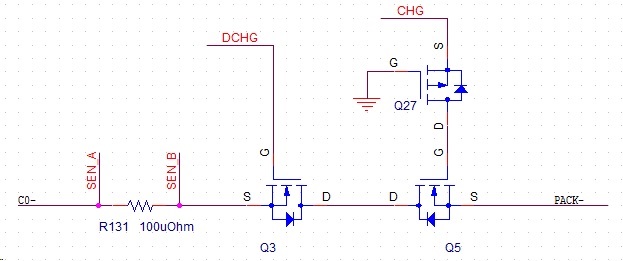
    UCC27524 is a good starting point for this application which will require a bias voltage of 18V recommended operating max, the dual channels may each drive CHG and DSG FETs as shown on your schematic. 

    Special precautions must be taken to prevent PACK- negative swings from reaching OUTx pins as the UCC27524 will not handle negative voltages exceeding -3V. The P-CH FET on Q5 is good starting point but i recommend adding additional resistors on Source and Drain of Q27 which might slow down a bit the turn-off sequence of Q5 but with 5-A drive current from UCC27524, it will be insignificant.

    Regards,

    -Mamadou   

  • Mamadou,

    Thank you for your valuable answer,

    1. Can you recommend alternate part with capability of handling -ve voltage to some extent? Is any other way i can protect the chip from damage due to -ve voltage ?

    2. May i know why the driver has more current rating when the FET can be turned ON with very few Charge ?

  • Wei Zhang, Thank you for your response meanwhile :)

  • Hello Tylor,

    1. UCC27524 will be the best candidate and your current setup with the P-ch FET between CHG gate and the driver OUT pin should protect the IC, I would simply add resistors on both Q5 gate and Source of P-ch as previously mentioned.

    2. The driver has a 5-A pulsed current capability to typically drive high gate charge FETs with short dv/dt at the gate to minimize losses in high switching frequency applications. For your case, though you might need such pulsed current, it may beneficial when driving several CHG in parallel with high gate charges to ensure fast rise/fall times.

    Regards,

    -Mamadou 

  • Hello Mamadou,

    Thank you for all your kind answer, Now we have more clarity on things which we doubted.

    Regards,

    Tylor