This thread has been locked.

If you have a related question, please click the "Ask a related question" button in the top right corner. The newly created question will be automatically linked to this question.

TPS61235P: Auto load detection circuit in power bank applications

Part Number: TPS61235P
Other Parts Discussed in Thread: BQ25895, , PMP4451, TPS61088

Hello TI team,

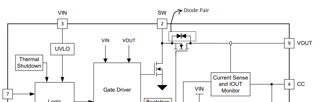
We are developing a power bank solution based around BQ25895 and TPS61235P ICs. We want to add auto load detection circuit to the output of the boost converter so that the power bank can remain in sleep mode unless a load is attached. We referred to the SLVA770 application note and found out a solution.

We also referred to PMP4451 reference design and it also had the same implementation. 


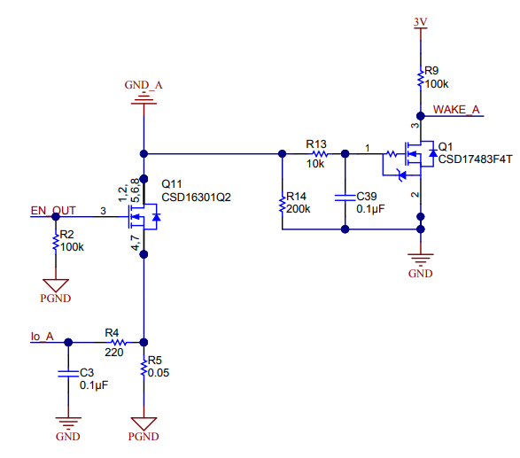
We implemented the same design using the same parts mentioned in the reference design. However, we were unable to get a logic low signal on the WAKE_A node when we connect a load to the design. At this point of time, the output of the boost converter is not enabled and the boost converter input is connected to a battery.

Following are the points that we would like you to elaborate on:

- what is the leakage current as mentioned in SLVA770 and where does it get generated?

- Are we missing something here?

Kindly let us know how to proceed forward using this design so that we can have a robust auto load detection logic in our product. Also, feel free to ask us any more information if required to help us solve this thing as soon as possible.

Regards,

Sarth

  • Hi Dave,

    I'll ask the reference design team to answer your question. Please wait a while.

  • Hi Dave,
        I will check with the related person about this. Because of the original designer was no longer in TI.

    Regards,

    Richard

  • Hi, Dave,

    Please make sure your schematic is the same as PMP4451 or SLVA770 mentioned circuit.

    The leakage current is generated like the following. Let me explain this referring to PMP4451 schematic. There is a default voltage on the boost output called Vo_BSTA or Port A VBUS pin even if boost is not enable because boost circuit diode can't block the battery flowing to its output. Note that at this time the voltage between Vo_BSTA and PGND is battery voltage(around 3.7V-4.1V) instead of Vo_BSTA and GND_A(when EN_OUT is not enable)

    1. Without anything on the port, there is no current path from VBUS to GND_A to PGND(GND_BSTA) because VBUS and GND_A is floating owing to turning off Q11

    2. When add a load on the port, there will be a [leakage current path from VBUS load, R14 and GND. Compared to R14 200kohm, the load is very small. that means the voltage of R14 will increase up to VBUS(battery voltage) quickly. once it exceed Q1 threshold, the WAKE_A will be low level.

    Based on the above logic, I recommend you checking the boost output voltage when it not activated. and checking the Q1 gate to GND after attached device on port A.

    Hope it will help, thanks.

  • Hello David,

    Thanks for the explanation. I think my understanding is proper relating to the functioning of the circuit and you response confirms it.

    However, when I measure the output of TPS61235P (boost converter) with its output disabled and battery attached to its input, I observe no voltage. Can this be because the TPS61235P has a blocking diode pair arrangement as described in its block diagram? (below image shows it marked)


    If this is the case then I believe that we cannot use the TPS61235P if we need to use the auto detection circuit or we need to find some other way? Is it correct?

    Regards,

    Sarth

  • Hi, Sarth,

    Yes, you are right. For TPS61235, in shutdown mode, a true disconnection between input and output is implemented. It can prevent current from input to output, or reverse current from output to input.

    In the PMP4451, it is using the TPS61088 for A port, there is no reverse blocking diode within it. 

    If you are using the TPS61235,  your understanding is correct.