This thread has been locked.

If you have a related question, please click the "Ask a related question" button in the top right corner. The newly created question will be automatically linked to this question.

LM5105: Propagation delay of falling edges changes at low duty cycle

Part Number: LM5105
Other Parts Discussed in Thread: LM5101, UCC27282, LM5106
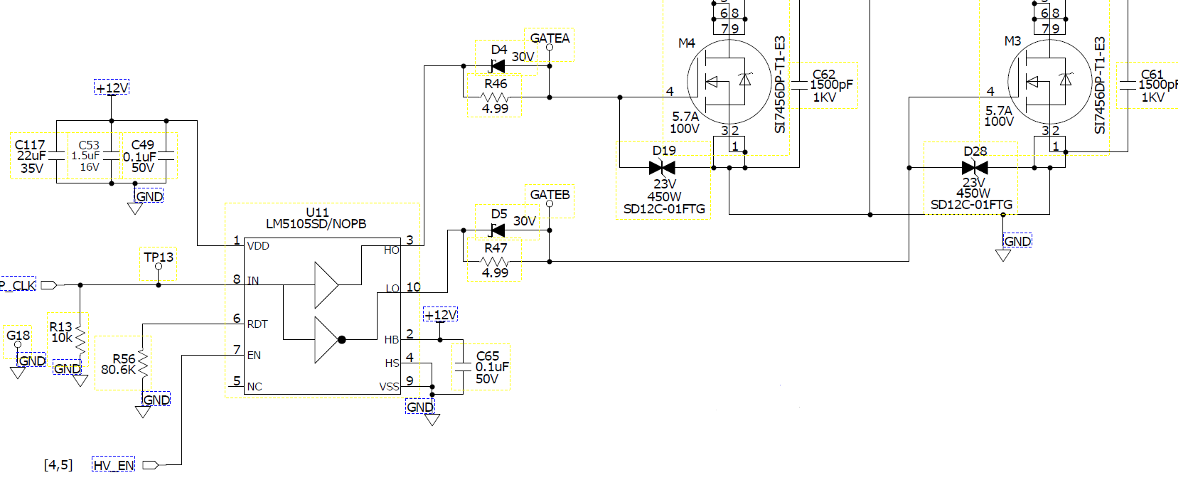
Basics:

Operating frequency is 125kHz

VDD and HB are +12V

Problem statement:

From 470ns to 520ns the falling edge of the clock tracks the falling edge of the HO pin with increasing propagation delay between them from 60ns to 68ns.  This isn't an issue for us and the result is nearly identical on the LO pin.  We aren't presently operating below 470ns.

Once you cross the 520ns threshold, the falling edge of the HO pin "snaps back" as seen in the video and you now have a constant propagation delay of 26ns for all increasing duty cycles.

This is an issue for us and causes severe instabilities in operation and loop tuning.

I have placed a video in here, but it doesn't look right.  Please let me know if you can't see it and how to get you the video.  I could create a dropbox link if that will work for you.

Additionally, I have limited the amount of data to you to help prevent info overload.  Please let me know of any additional details you might need and I will gladly try to provide them.

  • Hello Erik,

    Thank you for the interest in the LM5105. I was able to see the video, I think it had all intended content. I do have some questions.

    The channel 1 looked like it was significantly wider width than the other channel, I did see the pulse width jump on the second channel which has the narrower width and change in prop delay. If channel 1 in the IN signal, and the other channel is HO I would expect the HO to be close to the IN pulse width. Can you confirm the signals in the scope video?

    Also can you confirm the setting for the Rdt and the dead time you expect? It will help to see the IN, HO and LO zoomed such that you can see the dead times. Sweep the pulse width through the widths that you see the issue so you can confirm if the dead times are what you expect.

    Regards,

  • The channel 1 looked like it was significantly wider width than the other channel, I did see the pulse width jump on the second channel which has the narrower width and change in prop delay. If channel 1 in the IN signal, and the other channel is HO I would expect the HO to be close to the IN pulse width. Can you confirm the signals in the scope video?

    • Regarding this question, The signals are correct.  I believe it is causing confusion because of how tightly we are zoomed in.  If you look at the time scale you can see that we are at 40ns per division so the size of the pulses are a bit deceiving at first glance.
    • Ch1 is IN and Ch3 is HO.  The cursors on the screen have no value in the original video.  We should have turned them off along with Ch4.

    Also can you confirm the setting for the Rdt and the dead time you expect? It will help to see the IN, HO and LO zoomed such that you can see the dead times. Sweep the pulse width through the widths that you see the issue so you can confirm if the dead times are what you expect.

    • Regarding Rdt, our Rdt value is 80.6k.  When we measure the rising edge of IN to the rising edge of HO we see our expected deadtime plus rising edge propagation delay, that total time is 490ns as seen by the cursors in the new video .
    • As you have requested we have made another video.  In this video Ch1 is IN,  Ch2 LO and Ch3 is HO.  What we are attempting to show you is the (dead time + rising edge propagation delay) using the cursors. 
    • While showing HO and LO, we are driving IN's duty cycle up and down.  You can still clearly see what we are calling "A change in falling edge propagation delay" happen while the dead time remains constant.  We do not presently believe this shows a change in dead time, we do believe it is showing a change in falling edge propagation delay.
    • This problem is the same on both HO and LO.


  • Hello Erik,

    Thank you for the additional video, this does make it clear that the dead time looks like it is maintained.

    Were these scope plots taken with the driver and control only operating with low voltage, no power train high voltage input? It looks like this is the case. It appears the slight shift in pulse width and prop delay change happens not far beyond the HO minimum output pulse.

    Can you confirm a couple of things that may help. Confirm that the Rdt resistor is close to the IC connected with short trace lengths. Confirm that the VDD capacitor and boot capacitor are close to the IC with short trace lengths.

    Since the dead time is maintained at a fairly high value close to 500ns, I am curious how the slight timing shift is causing an issue in the power train. Is there a control point in the control loop which is complicated from the pulse width shift at a certain PWM input? Or is this causing a concern with the power train timing?

    Regards,

  • Hey Richard thanks for all the quick responses.

    Your welcome.  We thought the video showed it clearly also.

    Were these scope plots taken with the driver and control only operating with low voltage, no power train high voltage input?

    • Maybe the voltage scales are confusing the issue?  Do you mean is the IN signal level different from the HO and LO signal level?  On the scope they are at different scales.  IN is a 3.3V signal in our design as shown on the scope and HO/LO are 12V signals as shown on the scope. +12V is applied to both VDD and HB.  I'm not sure if this is what you are asking though so please let me know if that doesn't answer your question.
    • For this experiment, i.e. the scope videos, we disconnected the FETs so that the chip doesn't have to drive anything in order to prove to ourselves that it was purely related to the driver.  The problem perfectly replicates when the HO/LO are hooked up to the FETs they would normally drive.

    It appears the slight shift in pulse width and prop delay change happens not far beyond the HO minimum output pulse.

    • Can you help us, we are having trouble classifying what the "minimum pulse" of either HO or LO is based on datasheet specs.  We can see what it is in our circuit based on how we drive the duty cycle but we are wondering if there is a spec we are missing here.  

    Confirm that the Rdt resistor is close to the IC connected with short trace lengths.

    • Rdt is about .1 inch from pin 6 and attached to ground through a short .03 inch trace and via.

    Confirm that the VDD capacitor and boot capacitor are close to the IC with short trace lengths.

    • Boot strap and VDD caps are within .1 inches of pin 1 and pin 2.

    Since the dead time is maintained at a fairly high value close to 500ns, I am curious how the slight timing shift is causing an issue in the power train. Is there a control point in the control loop which is complicated from the pulse width shift at a certain PWM input?

    • Yes, this complicates our control loop at low duty cycles when running no load.  

    Our drive circuit actually perfectly implements the datasheet test circuit described above the 6.6 Switching Characteristics Table on page 6.  We don't actually utilize the bootstrap and just drive 2 low side FETs.  See attached image.  We detached the resistor and diode gate drive components for the scope videos we have made so far.


  • Hello Erik,

    You confirmed the questions I had. On the 1st question I just wanted to know if the scope plots were the driver only and not driving the power train, which you confirmed.

    On the second question, I am referring to the HO pulse width that initially appears with the increasing IN input width. It looks like the timing change happens not too much beyond when the HO starts switching.

    Thank you for confirming the close placement of components, and that you are using the driver only as two low side drivers and not in a half bridge configuration.

    I looked at my parts availability and I do not have the LM5105 available. It will take 3-5 days to receive so I cannot test the actual circuit until likely  Tues to Wed next week.

    I do have some things to try, depending on the minimum input pulse width that you desire/need in your application. In the controller when it is operating do you have a minimum pulse width that is much lower than the LM5101 will respond? It looks like the LM5105 starts the HO operation at ~460ns IN pulse width. Can the control signal have an IN input much lower than 460ns even though the driver and power train will not respond, this can also result in some possible control concerns.

    Can you try reducing the Rdt resistor to ~68K which will give a dead time of ~400ns, confirm if this is OK in the power train but this is still a conservative (long) dead time. Confirm the switching and timing of the LM5105 with this change, and see if the behavior is similar. I expect the IN pulse where HO responds to be shorter in this case.

    In the mean time I have the LM5105 devices coming to test when available if we have not resolved your concerns when they arrive.

    Regards,

  • Richard,

    We look forward to hearing how your testing goes!

    We will try your ideas tomorrow and reply back here with the results.

    Thank you for your time, patience and rapid responses.

    -Erik

  • Erik,

    Keep me updated when you get a chance to try the changes.

    Regards,

  • Richard,

    Here is a new video.  We have changed Rdt to 68.1kr as you requested.

    Based on our analysis of the change you requested, it appears that the change in propagation delay is staying referenced to either the end of dead time/beginning of the HO cycle or it is simply referenced to the rising edge of HO.

    -Erik H.

  • Richard,

    We have performed an additional experiment.

    Instead of changing the duty cycle of IN, we decided to modulate the enable pin to achieve our PWM and hold the IN clock constant, as a side note this also allows us to run independent duty cycles for HO an LO but that's a separate subject. 

    Results:

    1. When modulating Enable, everything works the same but we gain the benefit of non-complimentary HO and LO outputs.

    2. If we modulate the enable pin in phase with the rising edge of the IN clock signal the problem perfectly repeats.  This is not shown in the video below, just lettings you know.

    3. As an experiment we phase shifted our enable pulse to occur after all the dead time has elapsed to possibly gain some insight regarding what the shift in propagation delay is linked to.  In the video below you can look at the "cursors BOX" in the top right corer and see that the Cursor A is at 656.8ns, so a solid 150ns after deadtime, and cursor be is 28ns later.  we believe that 28ns accurately show the enable propagation delay.

    **We believe that the result of this experiment shows the HO falling edge propagation delay is physically tied to the rising edge of HO and doesn't change as we phase shift the enable pulse to occur after dead time has expired.  


  • Hello Erik,

    Thank you for the information, I will address your most recent post.

    Regards,

  • Hello Erik,

    Thanks for the update.

    One thing is not quite clear from your comments. When you hold the IN pin high and control the PW with the enable pin do you get the desired gate driver response you need? It sounds like that you see the non complementary LO and HO as a benefit. But it is not clear if this is a solution that works for you and does not have the pulse width shift that is a concern.

    I still need to look at the device next week when I get the material, but it looks like there may be a timing shift related to when the input pulse width exceeds the dead time plus maybe the propagation delay.

    I think when most applications are operating at 125kHz as you are, that the dead times are likely set much shorter. Or if long dead times are used it is likely in low frequency apps such as motor drive where the pulse widths are relatively long. I think in those situations this timing shift is likely not encountered.

    Regards, 

  • Richard,

    When you hold the IN pin high and control the PW with the enable pin do you get the desired gate driver response you need?

    • No we do not, the problem perfectly replicates when we use this alternate control scheme.

    It sounds like that you see the non complementary LO and HO as a benefit.

    • Yes it's a benefit, we came to use it because we were asked not to change the board at this time, so this works for us.

    But it is not clear if this is a solution that works for you and does not have the pulse width shift that is a concern.

    • This DOES still have the pulse width shift. 

    It looks like there may be a timing shift related to when the input pulse width exceeds the dead time plus maybe the propagation delay.

    • As we stated in the previous post, we believe that the result of the last experiment shows the HO falling edge propagation delay is physically tied to the rising edge of HO and doesn't change as we phase shift the enable pulse to occur after dead time has expired.  So looking at the video what you are seeing is:
      • CH4 is EN, CH1 is IN, and CH3 is HO
      • IN goes high then there's dead time, 400ns, then we wait an additional 256ns before we take EN high and the problem still occurs.  So on the scope you will see 656ns of delay from IN going high to HO going high and we are doing that by modulating the EN pin.

    I think when most applications are operating at 125kHz as you are, that the dead times are likely set much shorter.

    • based on our previous experiment where we changed to the new Rdt, we believe that the amount of dead time does not have any effect on the issue occurring.  It will always occur at the same amount of time after HO or LO go high.

    Or if long dead times are used it is likely in low frequency apps such as motor drive where the pulse widths are relatively long.

    • The error will always occur in our experiments so far but if you are only needing large duty cycles then you will not care about it.

     I think in those situations this timing shift is likely not encountered.

    • I am confused by your comment here.  We were certain that the video showing the result when we changed the dead time resistor as you requested clearly proved that you can't subvert the propagation delay by changing the dead time.  Somehow we have begun to miscommunicate.  Please re read the previous 2 post and watch the videos, then let us know if you would like us to restate something or perform a different experiment.  
  • Hello Erik,

    I wanted to confirm if the holding IN high and cycling EN provided better results, which you confirmed is not the case. I will look when I have the devices available next week.

    Regards,

  • Hello Erik,

    Getting the parts and the boards has taken longer than is typical, I still have not received as of Friday. I will confirm when I go to the office tomorrow.

    The other suggestion would be to determine the dead time that is adequate for the power train, as a minimum, and set the LM5105 for that deadtime setting and confirm if there is less propagation delay shift with increasing pulse width on the driver input.

    Regards,

  • Richard,

    Thank you for the thoughts.  We have tried a dead time as short as 100ns, but the shift in PWM still occurs shortly after the rising edge.

    -Erik

  • Hello Erik,

    I tested the LM5105 with slowly increasing IN pulse widths and observed the HO output pulse width shift (reduction) as the pulse width is increased, then the HO pulse keeps increasing with IN. I did try at various VDD to see if that made a difference and also with low RDT.

    For much more precise pulse width control of HO, or LO, to the driver inputs I would suggest the UCC27282 120V half bridge driver which has very good narrow pulse response and low pulse width distortion (input to output pulse width). This driver however is a two input driver so the HO and LO would have to be controlled with the LI and HI inputs. This would be the best option to have desired HO and LO pulse widths.

    There is the LM5106 which is pin compatible and similar function as the LM5105 but I do not know if part addresses the concern you have in your application. It may be worth testing this driver IC.

    Regards,

  • Richard,

    Thank you for the effort.  We had hoped there would be a fix but totally understand there isn't.  We will try the other parts in the design.  Thank you for you time.

    -Erik

  • Richard,

    We are excited to say that the drop in replacement, LM5106, is great and completely solves our problems.

    The shift in propagation delay is COMPLETELY gone and our supply output, previously clamped at 600V out, can now go as low as 20V out.

    This is so far proving to be a fantastic drop in fix and we can't say thank you enough for digging it up for us.

    Best of luck to you and we will update this thread if we discover any issues or surprises.

    Erik H.

  • Hello Erik,

    Thank you for the update and good news. It is good to hear we found a drop in replacement that resolves your issues, thank you for sharing that on this forum as it will likely be useful for other users in the future.

    Regards,