This thread has been locked.

If you have a related question, please click the "Ask a related question" button in the top right corner. The newly created question will be automatically linked to this question.

TPS548A29: Question

Part Number: TPS548A29
Other Parts Discussed in Thread: TPS548A28

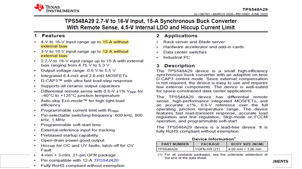
Datasheet show: 4-V to 16-V input range up to 15-A without external bias and 3-V to 16-V input range up to 12-A without external bias. why does the input voltage cause the output current  to change in different ranges? Could  you help me explain the problem? Thanks.

  • Hi

       Without external bias, the Vin is supplying the internal LDO which is used to drive the MOSFETs using the gate driver. A lower Vin, means a lower LDO voltage and thus lower gate drive. This means that the Rdson of the FETs could be higher and the lower current ensures that the FETs can handle the current at this Rdson.

    regards,

    Gerold

  •  

    Since the Gate Drive voltage for the TPS548A29 is derived from the input voltage when no external bias voltage is provided, the Rdson of the power FETs increases, reducing the over-current trip threshold and the range of application currents the device can support.  As a result, if an input voltage less than 4V will be supported, the load current should be limited to less than 12A.

    That is why, when an external bias of 4.75 - 5.3V is provided to support this gate drive and keep the MOSFETs fully enhanced, the rated load current is equal across the full range of load currents. 

  • Is there any relationship curve between no external bias voltage and Rdson?(The variation range of RDSON between 3v~4.5V) .Under circumstance of no external bias voltage, is there a relationship curve between temperature and Rdson, and output current?

  • The VCC voltage with no external bias for the TPS548A29 is 4.5V.  The external bias can only be 4.5V or greater.

    See Figure 13 and 14 in datasheet for the Rdson vs temperature.   

    Power dissipation in the IC will affect the device die temperature.   

    The input voltage, output voltage, switching frequency and output current affect the power dissipation. 

    See figure 3 to figure 5 of the SOA (temperature vs load current) area of the device for couple test condition.

  • Hi

    what is the any relationship between Vin(3V~4V) and Rdson under the no external bias voltage?(Rdson's data)

  • Hello, 

    Please see the TPS548A28 datasheet Figures 13 and 14 on page 10. 

    The TPS548A28 is similar to the TPS548A29.  The TPS548A29=8  hasVCC=3V  and the TPS548A29 has VCC=4.5V

  • Hello, 

    My question may not be clearly stated. What I want to consult is the 3V to 4V input range and without external bias, Rdson range?

  • We do not have this data. 

    The TPS54548A29 has a internal 4.5V VCC bias. 

    If the input voltage is less than 4.5V on the TPS548A29, the VCC voltage is ~VIN. 

    The TPS54548A28 has a internal 3.0V VCC bias.  

    The characterization data in the datasheets are using the external bias at 3.0V and 4.5V to measure the on resistance. 

    The on resistance with 3V internal bias is the same as 3V external bias.