This thread has been locked.

If you have a related question, please click the "Ask a related question" button in the top right corner. The newly created question will be automatically linked to this question.

TPS65296: :

Part Number: TPS65296

Hi,

I will be using a Xilinx MPSOC devices with a 32 bit-4Gb LPDDR4 device. Max bandwidth MPSOC can go is 2400Mbps. 

So basically I wont need 8A or 1.5A from both outputs of TPS65296 and I will be dependent on power calculators of my MPSOC and LPDDR. 

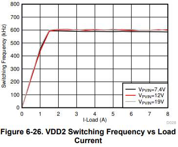
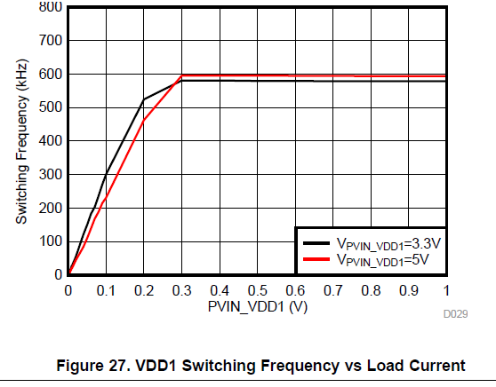
I see some graphs in TPS65296 datasheet shows the relation between, switching frequency-input power, switching frquency-load with certain input power etc.

I couldn't find TPS65296 in TI webench to make some simulations. 

My input voltage to TPS65296 for both Input pins will be 5V. Can you say by heart, this component is sufficient for me to use? 

Best regards

Onur

  • Hi, 8A or 1.5A means VDD2 8A, VDD1 1.5A?

    Yuchang

  • Hi, have you confirmed the current spec? Just would like to tell if VDD1 is 1.5A loading, this part can not support, if it is < 1A, you can just follow EVM BOM for design.

    Yuchang

  • Hi,

    Sorry for being not clear. I will use a 4GB LPDDR4 single 32 bit chip at 2400 Mbps(max) speed and an MPSOC.

    Because it is not an LPDDR4X I am not planning to use VDDQ output.

    Since it is just a single chip my current needs are much less than capability of TPS65296. FPGA current need from VDD2 is 135mA and from VDD1 it is 360mA. LPDDR4 power consumption summary is below. Should I still use the EVM BOM for my design?


  • Hi

        You will have to create the design for your current requirements as the EVM is designed for higher currents. The EVM design will still work at lower currents but it will be overdesigned for the currents that you are trying to use. Also, with such low currents, you might be in pulse skip mode, unless your inductor is large enough - which means that the ripple will be high. Can you please confirm what is the ripple requirements for these two rails as per the MPSOC?

    regards,

    Gerold

  • Hi,

    For 1V8 rail minimum voltage can be: 1.746V and maximum voltage can be: 1.854V

    For 1V1 rail minimum voltage can be: 1.06V and maximum can be 1.17V 

    Current needs for MPSOC at 1V1 is 135mA and 1V8 is 353mA

    Thank you in advance

    Onur

  • Hi, Based on your spec requirements, just follow EVM BOM is OK.

    Yuchang

  • Good to hear thank you. I will use the EVM as a reference.

    Is there a way that I can do simulation with my input voltage and load current for each rail? 

    Maybe in this component there are 2 buck converters already has TI manufacturing number that I can simulate individually?

    I also need to calculate the efficiency and power dissipation for my thermal simulation. 

    Thank you in advance

    Onur

  • Hi,

    I was checking the bom, all these capacitors and big inductor 744311068 is a bit overdesign for my application. Inductor: 680 nH with 17A spec with a very low DCR.  

    Is there anyway I can do a simulation with this component and instead of selecting all these components for 8A output, can I just adjust it?

    Instead of 74408943047 I am planning to use 7447786004. They are both 4.7uH from wurth and  first one has 2.2A with 45mohm DCR second one has 2.8A with 66mohm DCR. 

    Is there a way that I can do simulation with my input voltage and load current for each rail? 

    Maybe in this component there are 2 buck converters already has TI manufacturing number that I can simulate individually?

    I also need to calculate the efficiency and power dissipation for my thermal simulation. 

  • Hi, the 4.7uH inductor you will use is okay,  and since the current of VDD1/2 in your application is small, I believe the thermal is not a problem.

    Since there is no tool for efficiency and thermal evaluation, I suggest you can apply TPS65295EVM to do testing, 65295 is DDR4 solution, Vout is close to 65296, same internal logic and FETs, also you can apply 65296 samples and rework it on 65295EVM to use.

    Yuchang

  • Hi Yuchang,

    Yes I will be using TPS65295EVM, I am just wondering if I can also replace 744311068 (Inductor, shielded drum core, Superflux, 680 nH, 17 A, 0.0035 ohm, SMD) with another inductor since I dont need that much current in my application. 

    Except the inductors, I will use below schematic. I just wont populate 2 of the 22u output capacitors. I will replace 4.7uH with the one in my component database. Only open item now is to use 680nH 744311068 or not. Since I can not make a simulation, if you dont have a better(smaller) solution I would go with this big inductor.


  • Hi Onur,

    Yuchang is in day off today, so I'm not sure if he will reply and give the suggestion today. If not, he will give feedback next Monday. 

    From the perspective of the inductor selection principle, the overcurrent protection value is considered combined with the maximum loading current needs, since inductor saturation in OC may cause large peak inductor current. Except for the 8A loading in typical application, the 17A inductor is also chosen to cover the OC inductor current. So I think the current rating of the inductor cannot be too small.

    Yuchang is the owner of this device and familiar with corresponding solution. Let's wait for his suggestion.

    Regards,

    Andrew Xiong

  • Hi, Onur

    For VDD2 output caps, you can not stuff 2 of them but reserve the locations for backup, in my experience that should be Okay since your application current is small.

    For 680nH inductor, as Andrew mentioned, because the OC valley is around 10A, you can don’t use a 17A inductor but recommend the current ability can cover around 10A at least.

    Yuchang

  • Hi Yuchang,

    Thank you very much for your fast replies. I will let you know my final selection. Current baseline, I am using the same inductor from your Bom. 

    I have another question about the capacitors' voltage rating. What is the rationale behind 50V need? Is it because this is a generic design can also be used for other applications?

    Can I just use some other capacitors with lower voltage ratings that I already used in my design?

  • Hi Onur, sorry for missing your question, yes, you can use lower rating for these three parts, 50V is common P/N in my library.

    Yuchang

  • Hi Yuchang,

    Thank you very much for your support until this time. 

    I have another question regarding power-up and power down sequence.

    For power up and power down sequence, TPS65296 has internal solution by checking the VDD_EN pin. In case of uncontrolled power-down scenario, where do you think would be sufficient to add capacitors. 

    Do you have any study about this?


  • Hi, Onur

    I don’t fully get your mean, Do you mean add cap for EN? Generally only add nf cap to bypass high frequency noise. And Actually the power down of VDD1/2 also be controlled by IC itself.

    Yuchang

  • Hi Yuchang,

    TPS65296 has its own solution for ramp up needs of LPDDR4.

    I am looking for a solution for uncontrolled power-off scenarios for LPDDR4 device. Below picture is from Micron's LPDDR4's datasheet. So I need to keep VDD1 always greater than VDD2 even with uncontrolled power off scenarios.

  • Hi Yuchang,

    I know I am asking too many questions at the same time, sorry about that :) 

    We had discussed about my current needs are much smaller than what TPS65296 can offer. For my application, at some point, I wont even write or read from LPDDR so load current from both rails will be even less from the numbers I have shared earlier. 

    So from below pictures, Switching frequency will be less than 600 for VDD2 and less than 580 kHz for VDD1 in my application.

    I used almost the same circuitry from your evaluation board.

    Would this cause a problem? For 1V8, I think more or less my circuitry needs 300 mA but for VDD2 switching frequency will be much more less than 600kHz.

    My FPGA expects 1V1 rail in between 1.06V-1.17V 

    My FPGA expects 1V8 rail in between 1.746-1.854V

  • Hi, Onur,

    From power on/off timing(the picture you attached) in 65296, VDD1 always high than VDD2, not ony for ramp up but also for power down. I dont see any improper condition.

    For Frequency, it is no problem, since your current requirement is smaller, IC will enter PSM mode to save power and improve efficiency, Frequency will be reduced. it is OK.

    Yuchang

  • Good morning,

    All good news thank you. 

    I just wanted to be sure, if input voltage of the TPS65296 shuts off unexpectedly, would this cause a problem. 

    Even though we have an unexpected shutdown on input voltage of TPS65296, can we make sure while VDD1 and VDD2 are going off, VDD1 is always higher than VDD2?

    Thanks a lot.

  • Onur, Yes, in theory, it is yes. but if input voltage is power off, VCC is normal, even input voltage back to normal again, IC will not start up, because internal logic circuit works because of VCC ready, but no Vout since no input, then IC think the output is low and trigger IC UV latch off protection.

    Let's close this thread, if more questions, please send email to yuchang-zhang@tidotcom

    Yuchang

  • Hi Yuchang,

    I have sent an e-mail to your above e-mail last week. Do you think you could check it?

    Thank you in advance

  • Onur-san, sorry, I just checked seems i missed the Email, I will review and reply to you today by Email.

    Yuchang

  • Thanks, 

    I think you missed my last e-mail.

    Onur