This thread has been locked.

If you have a related question, please click the "Ask a related question" button in the top right corner. The newly created question will be automatically linked to this question.

TPS56628: TPS56628DDA 5V to 3.3V problem

Part Number: TPS56628

Hello everyone,

So I have an issue with the TPS56628DDA that I am using for my ckient's project: It is simply not delivering the voltage.

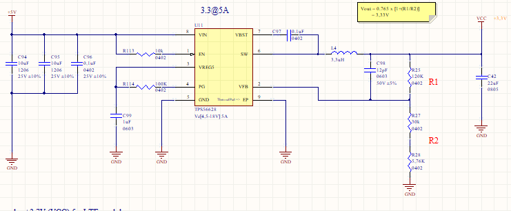
I am using this DCDC to convert VIN=5V to VOUT=3.3V and need up to 5A (more like 3A).

Here is the schematics that I have made:

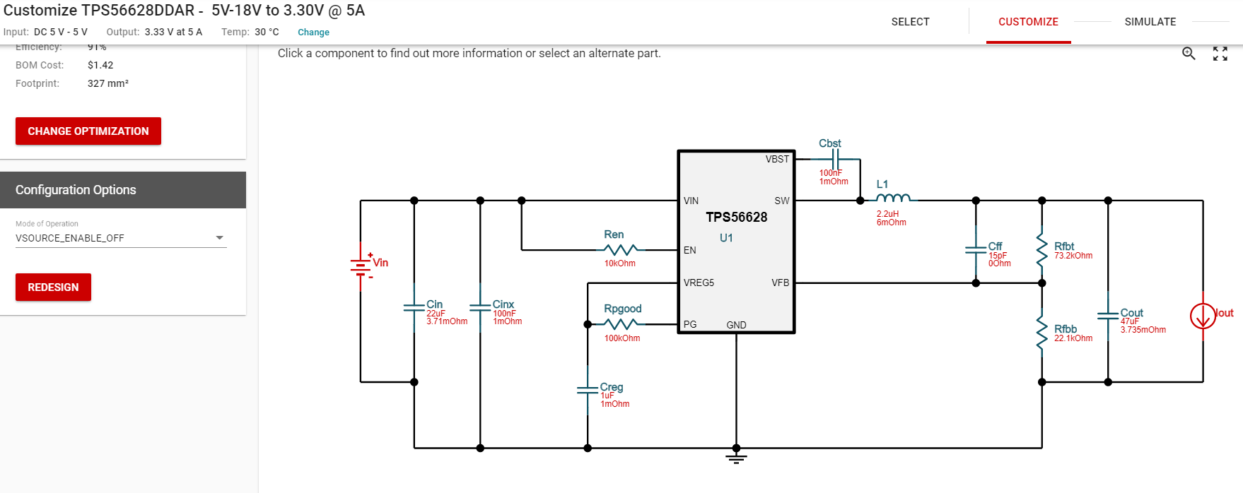
An here is the schematics form WEBENCH:

The voltage output that I am getting is 0.65V.

Can anyone please help? I don't really know what the problem is.

Thank you!

  • Hi, Seems can’t see your sch picture, can you re-upload?

    Yuchang

  • Hello,

    Yes sorry. Here are the schematics.

    My circuit:

    WEBENCH Circuit:

    Thank you.

  • Hi, schematic looks well, just suggest to add one more 22uF output cap, and this should not cause no Vout.

    Did you check Soldering? And how many boards did you test? Are they same result?

    Did you test the VIn/EN/VReg5/SW waveforms?

    And also Please capture your layout pictures for reference.

    Yuchang

  • Hello Yuchang,

    First, thank you for your help!

    Here are my answers:

    1-Did you check Soldering? Yes soldering is fine

    2- And how many boards did you test? Are they same result? We have 4 boards, but there is a modification we have to make before the board works. We did it for one board, but not yet for the others. Once it is done, we will test the other boards too

    3- Did you test the VIn/EN/VReg5/SW waveforms? So the boards are at my client's, so I don't have access and they don't have an oscilloscope (sorry). But I did get the values

    - VIN=5.07V

    - EN = 4.94V

    - VREG5 = 5.03V

    - PG= 0V

    - SW= 0.64V

    - VBST=5.7V

    - VFB = 0.16V

    4- And also Please capture your layout pictures for reference

    I am thinking that the problem might be in the startup of the DCDC, but we obvioulsy need an oscilloscope to check that. So I will be able to check it when the client sends me a board to test on my own (or if they buy an oscillo).

    Thank you again.

    Best regards,

  • Hi,

    Layout is really not good, especially for the input and Ground. My suggestion is

    For layout

    You can try to jump short and strong wire line from GND pin to output cap GND and input cap GND. If thermal pad can be connected, it is better.

    Make input line stronger, the line from input cap to pin is narrow and looks it is only one via connected to 5V? If so, jump a strong wire line to 5V from the input cap directly.

    For waveforms

    VIN/SW/Vout still need to be tested

    Yuchang

  • Hello Yuchang,

    Thank you for your help.

    For the Ground, just a clarification. Apart from the GND internal plane, there are GND polygones recovering the whole board (as much a possible) both on the TOP and BOTTOM side that are not shown in the image. But I guess it  is more for shielding purposes.

    We will try this solution in the next few days, I'll post back the results, and the waveforms when we get them.

    Thank you again!

    Best regards,

  • Hello again,

    So I finally found the problem. It wasn't actually on the circuit of the DCDC but rather after that.

    There was a Zener diode after the circuit at the filtering block of the component that uses VCC, and it was mounted inverted. So now that is fixedand  it works.

    But I will anyway put a wire at least between +5V and the input cap to try and avoid problems when we put full load on that VCC.

    Thank you for your time and your help!

    Best regards.