This thread has been locked.

If you have a related question, please click the "Ask a related question" button in the top right corner. The newly created question will be automatically linked to this question.

UCC28950: UCC28950

Part Number: UCC28950
Other Parts Discussed in Thread: TINA-TI

SINE WAVE OUTPUT INVERTER ASSEMBLY:  FULL BRIDGE MOSFET CONTROL SYSTEM

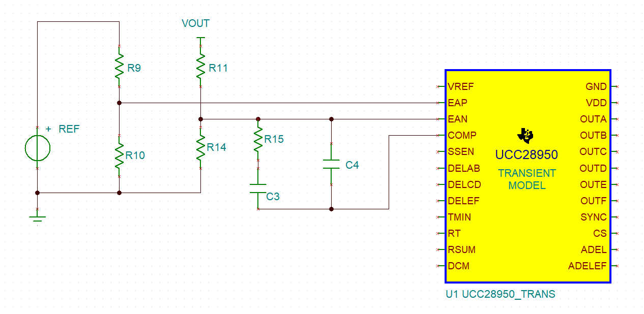
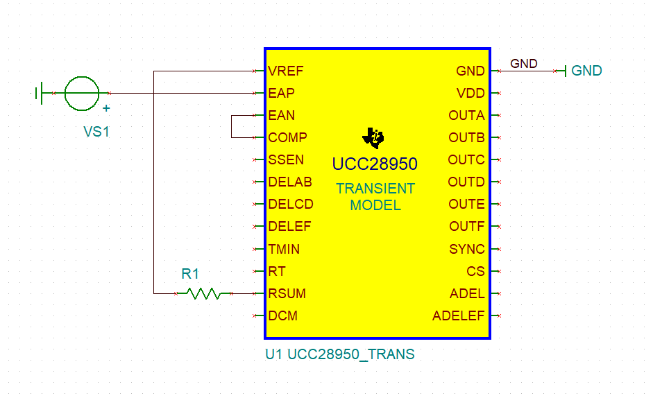
OKAY WHAT IM TRY TO FIND OUT  IS THAT CAN YOU GET THE DEVICE TO PRODUCE A CLASS-D OUTPUT DRIVE SIGNAL'S . NORMALLY YOU WOULD SET THE + INPUT OF THE ERROR AMP WITH A DC REF VOLTAGE AND YOU SHOULD SEE THE OUTPUTS OF THE DEVICE AT 50% DUTY CYCLE SQ WAVE AT THE SWITCHING FREQ. NOW WHAT I WONT TO DO TO PRODUCE THE CLASS-D OUTPUT DRIVE SIGNALS S TO SET UP THE OSC TO SWITCH AT 52KHZ ARE USE A EXT CLOCK IN , SO NOW I HAVE A RAMP SIGNAL PRESENTTHEN I WILL SET THE +INPUT OF THE ERROR AMP WITH +2.5 VDC,THE - INPUT TO THE ERROR AMP IS STILL OPENNOW I SHOULD HAVE OUTPUT DRIVE SIGNALS AT 50% DUTY CYCLE NOW ON THE ERROR AMP COMP PIN #4I INPUT A LOW FREQ SINE WAVE AT LETS SAY 400HZ AND 2V PK-PK. NOW I SHOULD SEE THE OUTPUT DRIVE SIGNALS CHOPPED TO REPERENT THE SINE WAVE IN,AND THEN I CAN ADJ. THE SINE WAVE TO GET THE BEST OUTPUT SIGNAL BEFORE CLIPPING THE RAMP SIGNAL, THEN I WILL USE A PRECISION EXT. OPAMP AS THE FEEDBACK ARE ERROR AMP CONTROL WHICH IT WILL HAVE A +2.5VDC REF ON THE + INPUT OF THE EXT. AMP. THE FEEDBACK SIGNAL WILL BE A SINE WAVE INPUT THE SAME AMPLTD. AS THE SINE WAVE REF SIGNAL ON THE COMP. PIN TO SET THE FINIAL OUTPUT VOLTAGE. SO AS I LOAD THE OUT PUT IT WILL MOVE THE PHASE CHANGE TO COMPENSATE AND KEEP THE OUT TO MATCH THE SINE WAVE REF. ON THE COMP PIN.

TAKE A LOOK AT THE DATA SHEET ON PAGE #16 FUN. BLOCK DIAG. AND LET ME NO IF I'M CORRECT

THANKS YOU,

WILLIE L. MCCAIN

wmccain@mccainlab.com

561-846-0150

  • Hello Willie,

    Thank you for your interest in the UCC28950 PSFB controller.

    I don't know the answer to your question myself, but let me connect you to someone whom I believe can help you.

    Regards,
    Ulrich

  • Hello Willie,

    This is a unique use for the UCC28950 and I don't know if you can get it to work as a class D amplifier.

    The UCC28950 is phase shifted full bridge controller drives and HBRIDGE.  Keeping the A and B switching operating 180 degrees out of phase and synced to a master clock. The C and D switched are also operated at 180 degrees out of phase and are phase shifted with the master clock to control the affective duty cycle.  The following link will bring you to an application note that shows how to design with this controller and how it operates in a PSFB, which is generally used for 500W to multi kW designs.  You might want to review this to see if this device might have a possibility of running  in your application.  

    From your question it sound like you are trying to design a Class-D audio amplifier.  The following link will bring to a TI webpage that discusses how to accomplish this with TI devices.  This is not my area of expertise.  However, I think you will find this link useful. 

    Regards,

    Mike

  • NO THIS IS NOT A CLASS-D AMP 

    ITS A HI-OWER SINE WAVE  INVERTER, I KNOW WHAT THE PART CAN DO 

    I NEED TO NO IF I CAN USE A sine wave to modulate the output

  • i need some one to think out side the box on this and stop running ,look at the part and let me no if by using a sine wave you can get the output to modulate.

    so first you set the part up for a hi freq carrier let say 50khz to 100khz this will act as the carrier , now at this point you will have 50% dc sq. wave out , now what i wont to do is palce a sine wave of approx 2v pk-pk on the comp pin may be with a 1k ohm resistor in series just to add a buffer,wait no!  not a resistor a cpacitor at 1 mfd this will give islation for the sine wave and allow it loat on the ref dc voltage form the op amp and anyother off set internal to the chip.the + input of the error amp will have a +2.50 vdc ref the - input of the error anp is still open , now you slowly start to apply the sine wave and watch to see the output modulate to the low freq. sine wave ref at 400 hz

  • Hi Willie

    I'm not completely clear as to what you want to do but here goes anyhow.

    If you want your sine wave inverter to produce an output without a DC offset - ie, equal positive and negative amplitudes - then the PSFB is the wrong topology and so the UCC28950 won't work in this application. The reason is that the PSFB is a single quadrant output topology - pos Vout, Pos Iout or neg Vout, Neg Iout but not both at the same time. If this is what you want then you should look at the apps note that Mike linked.

    If you want the sine wave inverter to produce a unipolar output that is modulated by a 400Hz sinewave then it can be done. I've never seen this done in practice but here's the general idea...

    Normally the output voltage is determined by the reference voltage fed into the error amplifier. A DC reference gives you a DC output, a varying reference gives you a varying output. The general arrangement is to modulate the reference (EAP) rather than the output of the error amplifier (COMP). Some caveats apply

    The output will follow the input provided that the loop bandwidth is sufficiently higher than that of the modulation - if you are using 400Hz this won't be an issue because it's easy to achieve 5kHz or even 10kHz loop bandwidth - especially if you are using peak current mode control.

    You can expect some distortions in the output sinusoid at no load or under light load conditions because there is no load available to discharge the output capacitance as the modulator tries to lower the output voltage.

    The duty cycle will be limited to about 15% to 85% (roughly) - this will affect the depth of the modulation you can achieve - especially at the low end.

    Regards

    Colin

  • DONT WORRY ABOUT THE DC OFSET THATS THE EASIEST PART TO DO THATS NOTHING

    AND DONT THINK IT CANT THINK IT COULD YOU HAVE TO GET IN THERE STOP RUNNING.

    No!

    Here is the setup.

    Note: remove all the components you have laid out, start over.

    Now,

    1)TAKE A 1 MFD CAP PLACE ONE END TO THE COMP PIN, THE OTHER END THIS IS WHERE THE 400 HZ SINE WAVE WILL GO FOR NOW SET TO ZERO.

    2)FROM THE REF PIN USE 2/ 5.1K RESISTORS IN SERIES THIS WILL PROVIDE THE REF VOLTAGE TO THE +INPUT OF THE ERROR AMP.

    3)SET THE MODULATOR UP TO LET SAY 52KHZ, THIS WILL ACT AS THE CARRIER FREQUENCY.

    4) NOW AFTER ALL OTHER PINS HAVE BEEN SET UP AS REQUIRED THE UNIT SHOULD OUTPUT SQ. WAVE DRIVE SIGNALS ( CORRECT! )

    5) I WILL BE USING ( RSUM PIN ) AS MY VOLTAGE FEED FORWARD FOR THE BUS SENSE LINE.

    NOTE: NOW LOOKING AT THE OUTPUT DRIVE SIGNALS SLOWLY START TO INCREASE THE SINE WAVE REF SIGNAT AT 400HZ AND SEE IF THE OUTPUT SQ WAVE START TO CHOP AT THE 400 HZ REF SIGNAL AND SEE WHAT THE AMPLT. IS WHERE THE INPUT SINE WAVE STARTS TO CLIPP THIS IS PROBERLY WHERE THE OUTPUT DRIVE SIGNALS GO BACK TO A FULL SQ WAVE AGAIN.


    WHAT I’M TRYING TO DO IS SEE IF I CAN GET THE OUTPUT SQ WAVES TO MODULATE AND CARRY THE LOW FREQ SINE WAVE ACROSS THE POWER MAGNETICS, WHERE NOW THE HI-VOLTAGE MODULATED SQ WAVES WILL GO INTO A LOW PASS FILTER AND THEN I WILL RECOVER THE 400 HZ SINE WAVE BUT NOT AT 115 V RMS AT HI CURRENT.


    LET ME NO

  • Hello Willie

    The output of the error amplifier of the UCC28950 cannot be used as an input so you won't be able to feed a signal onto it whether you couple it through a capacitor or not. If you want feedback from the output then the correct method is to configure the error amplifier as I have shown above. If you want to run the system without feedback then configure the error amplifier as a unity gain follower by tying EA- and COMP together and feeding the control signal onto EA+.

    I'm still not sure what you want to do but you can simulate it using TINA-TI Texas Instrument's free pspice simulator - you can find it at https://www.ti.com/tool/TINA-TI

    Regards

    Colin

  • OKAY I UNDERSTAND AND YOU ARE CORRECT WHAT I WILL DO IS USE THE ERROR AMP AS A BUFFER INPUT FOR THE SINE WAVE SIGNAL , NOW WHAT IS THE SIZE OF THE RAMP ,AND IS THERE A WAY I CAN INSERT A TRUE TRIANGLE WAVE INTO THE PART BECAUSE THE SIZE OF THE RAMP ARE TRIANGLE DETERMINS THE GAIN OF THE SYSTEM 

    1) LET ME NO WHAT THE OFFSET VOLTAGE TO BE FOR THE SINE WAVE ARE CAN I USE =2.50 vdc ?

    2) WHAT IS THE SIZE OF THE RAMP ,AS FAR AS PEAK AMPLTD?

    3)NOW BASED ON THE OFFSET OF THE RAMP IF IT 100MV 500MV LET ME NO AND IS THIS WHERE THE SINE

    WAVE BOTTOM SHOULD BE AND THE TOP SET TO THE PEAK OF THE RAMP THIS WILL BE MY PK-PK SINE WAVE LEVEL?

    4) NOW I WILL USE A EXTERNAL ERROR  AMP BY TI AS THE FEEDBACK ,ARE ERROR AMP SO ON THE + INPUT THIS IS WHERE I WILL HAVE THE SINEWAVE REF,A FIXED IGNAL NO HIGHER THAN THE PEAK OF THE RAMP, THE

    NEG. INPUT WILL ONLY HAVE THE DC VOLTAGE REF ON IT NOW AT THE OUTPUT OF THE ERROR AMP INTO THE UCC PART THE SINE WAVE SHOULD BE THERE RIDING ON THE OFFSET VOLTAGE ,NOW AS I START TO INCREASE THE SINE WAVE ON THE NEG. INPUT ONCE I MATC THE REF THE OUTPUT SINE WAVE INTO THE UC PART SHOULD START TO DECREASE IN AMPLTD CORRECT?

    5 I NEED TO NO IF I CAN INSERT A EXTERNAL TRIANGLE WAVE NTO THE PARTTO GET MORE GAIN?

    THANKS FOR ALL YOUR HELP

  • I SEE THAT THE UNIT HAS A OFFSET OF 800mv

    ramp peak = 2.8vdc

    error amp has a offset of  250mv

    error amp out max is 4.25 vdc

    so now this means that i should set the external error amp with+2.25vdc this will be my center for the sine wave to ride on and the sine wave has  2v pk-pk range, now on the neg input of the error amp i will have the same , so when i load the out put if the voltage drops the sine  will increase if it over it will decrease to maintain the output the same, this should work correct?

  • Hi Willie

    I think so but let me consider this a little bit more and I'll get back to you - maybe today, if not then tomorrow.

    Regards

    Colin

  • Hi Willie

    If you configure the UCC28950 for Voltage Mode Control then the two inputs to the PWM comparator are the COMP signal and the internal RAMP. You then get a duty cycle which is proportional to the voltage at the COMP pin - with the offsets you mention. The RAMP input is an internal fixed one and isn't adjustable, other than for frequency.

    Connecting the RSUM pin to VREF puts the controller in Voltage Mode Control. The value of RSUM sets the slope compensation ramp but this is not used in VMC except in the case of current limit which isn't applicable in your case but it must be within the limits in the data sheet in any case so I'd set RSUM to 100k.

    In this configuration, the duty cycle will be proportional to the voltage at the EA+ pin (VS1). The characteristic will be 0.8V < VS1 < 2.8V to get a duty cycle between 0% and 100%. As I mentioned previously there is a Dmax of about 95% (at 100kHz) and the TMIN value will set a minimum achievable duty cycle.

    The gain of this system is fixed by the interal ramp - there isn't anything you can do with it. If you need variable gain then you will have to use the external source to provide it.

    There is no voltage feed forward either - except of course that you could again configure the external amplifier to provide it.

    Regards

    Colin

  • OKAY MR GILMORE

    IM CLEARING UP THE PICTURE NOW YES I UNDERSTAND,NOW THE VOLTAGES I GAVE WAS THE OUTPUT VOLTAGES OF THE ERROR AMP FROM 2.50V TO 4.24VDC CORRECT?

    BUT YOU ARE SAYING THE INPUT TO THE ERROR AMP + PIN NEEDS TO BE FROM 800mV TO 2.80VDC CORRECT?

    SO THEN MY CENTER WILL BE 1.80VDC REF AND MY SINEWAVE WILL HAVE A PK-PK LEVAL OF 1.6VPK-PK THAT WILL RIDE ON THE DC REF VOLTAGE TO MODULATE THE DEVICE CORRECT.

    RSUM, SO THE VOLTAGE ON RSUM NEEDS TO BE STABLE THAT WHY ITS CONNECTED  TO V REF ARE CAN I USE A VOLTAGE DIVIDER FROM THE BUS VOLTAGE AND SET THAT TO BE A AMOUNT IN NORMAL OPERATION AND AS I GO TO OVER VOLTAGE THE VOLTAGE WILL BE JUST UNDER 5 VDC, BECAUSE I DONT SEE ANY DATA ON THE RSUM PIN OTHER THAN HI = VOL AND LOW FOR CURRENT MODE, BUT WHAT LEVEL IT NEEDS TO BE AT FOR VOLTAGE MODE IN min  VALUE.?