Hello team,
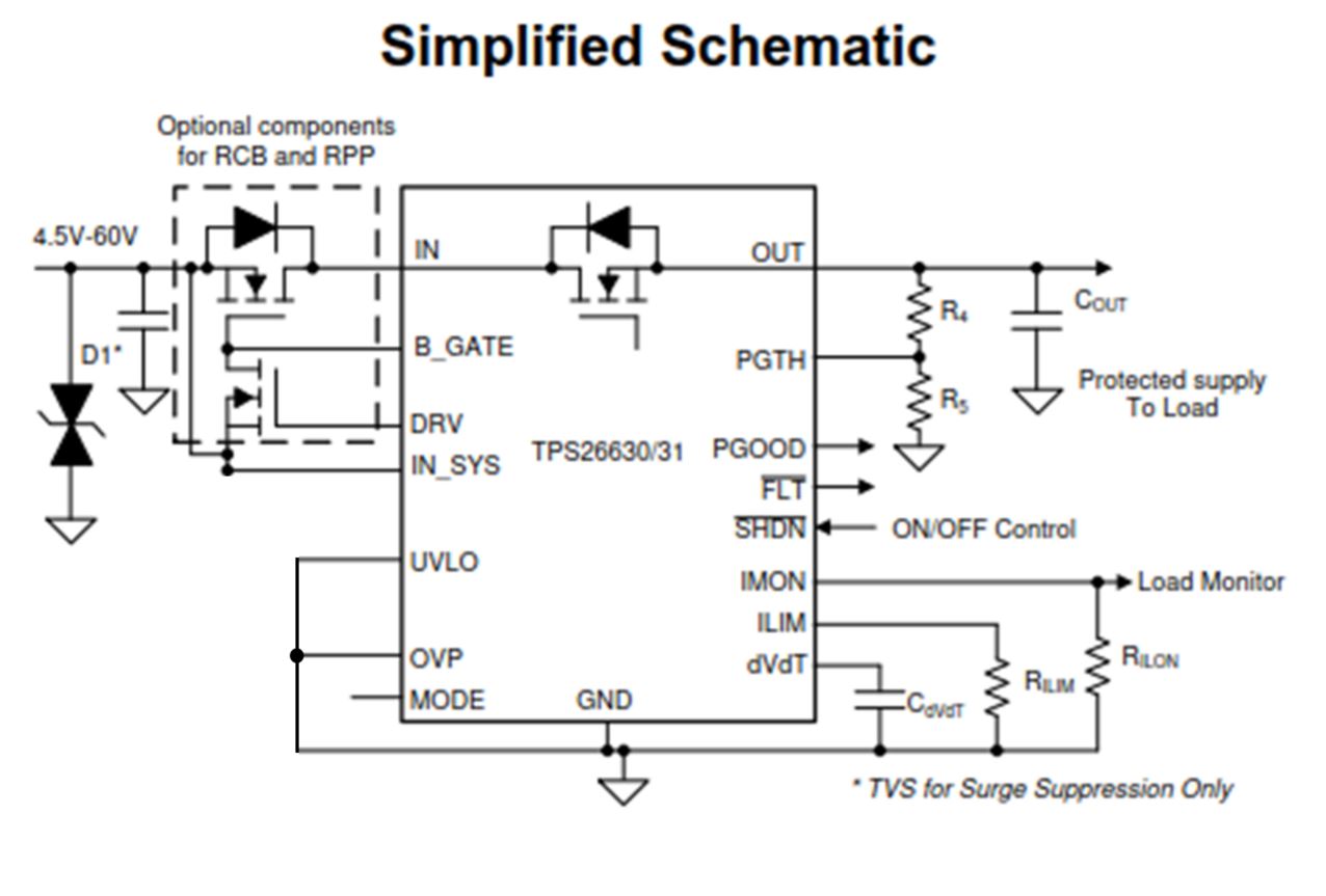
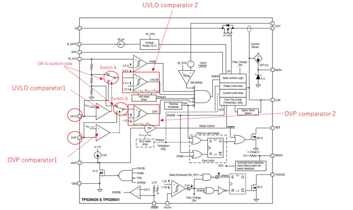
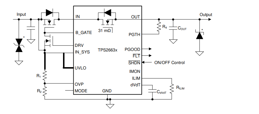
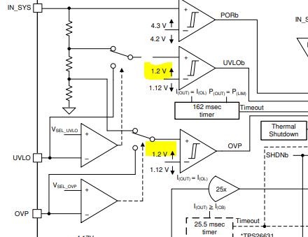
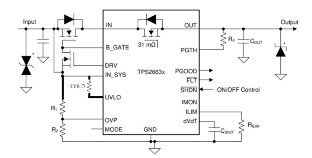
Customer will not use the functions of UVLO and OVP.
Could you advise how customer should treat the pins ?
Thank you and best regards,
Michiaki
Hello team,
Customer will not use the functions of UVLO and OVP.
Could you advise how customer should treat the pins ?
Thank you and best regards,
Michiaki