This thread has been locked.

If you have a related question, please click the "Ask a related question" button in the top right corner. The newly created question will be automatically linked to this question.

TPS92691-Q1: Damage on TPS92691-Q1 during LED current at 3A or more

Part Number: TPS92691-Q1
Other Parts Discussed in Thread: TPS92691

Hi,

I am using TPS92691-Q1, seeking advise for this problem
( 5 times) encounter this chip damage as well as switching MOSFET damage when I increase LED current to 3A or more.
( I increase LED current by varying pin6(IADJ) voltage using a benchtop PSU ).
( Voltage input setting to 40V )
the damage is in not immediate, but only after about 3 mins.

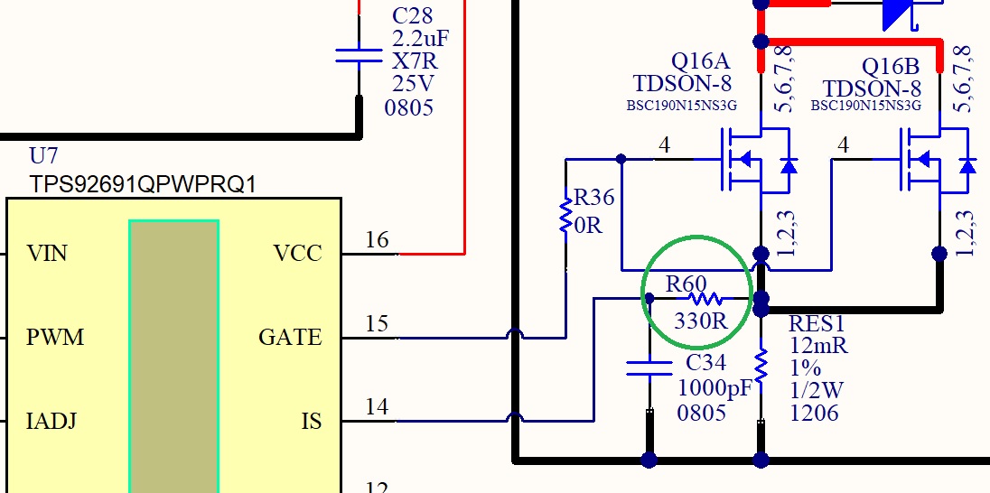
below are some of my buck-boost configuration
( LED max current is 4.2A , 36V forward voltage )
( input voltage range = 32 to 54.6V )

1: dimming control PWM(pin4) and DDRV(pin11) are not used
2: switching frequency is 80kHz , pin3(RT) resistor = 105K ohm
3: pin2(SS) CAP 0.047uF
5 pin5(comp) (2.26Kohm in series with 0.068uF) + parallel 750pF
6: 2 switching MOSFETs (in parrallel) using infineon BSC190N15NS3 G (Id(max)=50A, VDS = 150V )
7: switching sense resistor (at IC pin14(IS)) to Ground) = 12m ohm (1/2W)
8: Power inductor = 22uH (coilcraft MMS1210, 8.8A (Isat) )
9: LED current sense resistor = 20m ohm (1W)

  • Hello,

    We will need a schematic from you.  In addition, I want to verify that the max input voltage is 54.6V, the LED forward voltage is 36V.  Can you monitor the temperature on the FET's to see if it's getting hot.  I want to verify that you have adequate heat sinking for the FET in your board layout.

    Thanks Tuan

  • Hi,

    Attached is the schematic.

    Max input voltage is 54.6V. Yes. ( design for Li-ion cells of 13 S : 4.2 x 13 = 54.6 )

    LED forward voltage ( according to LED spec) possible up to 40V, but so far my measurement (at 25°C) is 36V at 4.2A

    I have not measure the MOSFET temperature yet, ( will do so later when more of the TPS92691 chip is delivered to me).

    the 2 MOSFETs is SMT package, so heat dissipation depend on the TOP and BOTTOM copper plane

    another problem I want to state is that,

    I have to add a 330 ohm resistor between C34(U7 pin14) and RES1 ( at the Source of the MOSFET Q16A/B )

    else ( as in the schematic without 330 ohm ), the close loop control will be lost when current is increase above (about) 3A.

    Thanks

    Tioh

    TPS92691-Q1.pdf

  • Hi Tioh,

    Why are you adding that a 330 Ohm resistor for.  Is the RIS (RES1) also damaged? 

    Just a quick calculation shows that the power dissipation on the power stage:  The output power is about 36V x 4.2A = 151 W.  Assuming roughly 80% efficiency you will have about 40W dissipation on your FET's, inductor and output diode.  it might be hard to remove this 40 W power with ground plane of your board.  My guess is that that the FET's are getting hot and gets damaged and that's what is taking out the TPS92691. 

    The IS feedback should have a 330 Ohm resistor between the RES1 and C34 with C34 near the TPS92691 and that form a RC filter before feeding back to IS otherwise you can falsely sense IS.

    Thanks Tuan

  • Hi Tuan,

    Thanks for your info.

    I will focus on studying the FET heat dissipation.

    Regarding the 330 ohm resistor, Yes, the placement of this resistor is exactly as what you have described, between RES1 and C34 ( as shown in the attached picture below, "R60" )

    I realized adding this resistor is necessary if the LED current is adjusted to more than 3A, else the buck-boost cannot maintain the close loop control ( if without this 330 ohm ).

  • Hi Tioh,

    Yes, you need that resistor and it's in the right location.  I'll will close this thread now and you can open another one if you have any more questions.

    Thanks Tuan