This thread has been locked.

If you have a related question, please click the "Ask a related question" button in the top right corner. The newly created question will be automatically linked to this question.

LM25145: switching waveform

Part Number: LM25145

Hi,

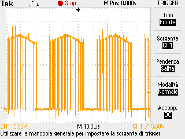
after struggling for having correct regulation with my LM25145 buck converter board, i finally got right regulation, also with load, and i can achieve 12V from 24V input. My question is, if this waveform i have at switching ndte it is correct. I don t understand why there is a ~9us hole (0V signal) in switching waveform, every ~32us. Is this a normal behaviour?? Or is this a weird switching waveform?? I also can hear a loud noise coming out from regulator, similiar to a whistle.

Someone who has experience with switching buck regulator, can give a little assessment? Many thanks.

Kind Regards

Emanuele P.

  • sorry i forgot to post image:

  • Hello

    The wave form does not look correct.

    Please send you schematic and a view of your PCB layout.

    I will assign to my colleague.

    Thanks

  • Hi Emanuele,

    At first glance this looks like compensation instability.

    Can you fill out a LM25145DESIGN-CALC with your values and attach it here?

    If it is not the compensation values then it may be layout related.

    Let me know,

    -Orlando

  • Dear Sir,

    If you could explain according to your experience why this waveform is not good, it will be very appeciated.

    if you could just give a hint about how should be a correct waveform, this is enought. Schematic review is not needed. Thanks for the infos

    Kind Regards

    Emanuele Peruzzi

  • Emanuele, 

    That SW node waveform is unstable, I can see the OFF time is varying alot and the switching frequency is probably not constant.

    Most likely output voltage ripple is very large.

    A good SW node waveform would have constant frequency with consistent ON-time and OFF-time.

    See figure 64 in the LM25145 datasheet.

    Please fill out LM25145DESIGN-CALC so we can troubleshoot.

    Orlando

  • Dear Sir,

    after some days struggling with board, it turned out that regulator or Q2 low fet, or both were damaged, changing both solved the problem. Now i can see a clear SW waveform, stable in duty and amplitude.

    In addiction i also found that i had source power supply (the external +24V) Vin, coming from a bad regulator, wich has stability problems, this led to a big oscillation in regulated output (almost 1V p-p). 

    I still have some difficulties to understand what caused damage to components, why regulator or low fet broke. Can i ask for a layout review, i already posted layout in another post, https://e2e.ti.com/cfs-file/__key/communityserver-discussions-components-files/196/LM25145_5F00_12V_5F00_reg.zip. I have a doubt in layout, i'm quite sure that fets, inductance and Cout are correctly placed, according to snva803 document, figure 3, vertical layout. But my layout has input capacitance Cin in a different place, i don t undestand if this difference could lead to stability problems. Please have it a look,

    Thank you for kindness,

    Emanuele Peruzzi

  • Hi Emanuele,

    The input capacitance should be closer to the FETs, these capacitors supply the switching current the the high frequency power loop and if they are far away you are introducing undesired parasitic inductance.

    Please see section 11.1.1 of the LM25145 datasheet.

    The SW node would have spiking due to inductance introduced to this loop. What does your SW node overshoot/undershoot look like?

    Maybe that is what damaged your first design, but I am more likely to believe the bad power supply was causing instability.

    -Orlando