This thread has been locked.

If you have a related question, please click the "Ask a related question" button in the top right corner. The newly created question will be automatically linked to this question.

question about UCC27322

Other Parts Discussed in Thread: UCC27322

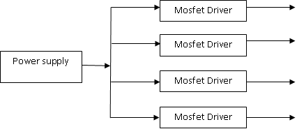
32 Mosfet drivers have been used as 32 liner drivers, the frequency of line driving is 2MHZ, the capacitance of each load is 200pf and the power supply is 15V.

Based on those data, the min power needed is P = 32 x f x C x V x V = 56watt and the current supply is 3.75A.  

Since each Mosfet driver can sink 117mA current, the rising time of output wave would be trise = (C x V) /I = 897ns.

My question is all those 32 Mosfet drivers share the same power supply, how I can make sure each Mosfet driver can sink the same current?

Can I use current limiting circuit or use any commercial chips from TI?


  • Any suggestions?

    Thanks.

  • David,


    The power you calculate is the average power which you use to rightly specify your required power supply for your circuit. However the sourcing and sinking of the drivers is a lot greater than 117mA. In fact the UCC27322 can source up to 9A for short periods of time. this instantaneous current would be sourced from the local capacitor on VDD of the driver. The capacitor value would be based on the gate input capacitance, driver source current and acceptable voltage dip on VDD (maybe 0.5V to 1V).To reduce this current level you could add gate resistors to each MOSFET, but this will slow down the turn on and turn off of the MOSFETs, which will cause significant losses since you switch at 2MHz.


    Hope this is of some help.


    Reagrds,


    richard.

  • Please let me know do you have reference design for selecting those local capacitors.

    Very appreciate for your generous helps.

    Many thanks.

  • David,


    I don't have a reference design but the process would be:


    1. estimate the rise time of the MOSFET, tr = Ci x Vg / i_drv = 200pF x 15v / 4.5A (9A for a short period) tr = 667ps

    2. Calculate minimum VDD capacitor, C_VDD > tr x i_drive / dV, (dV allowable ripple on VDD) C_VDD > 667ps x 4.5A / 0.5V = 6nF, use 10nF per driver. In fact the driver data sheet recommends 1uF at VDD (pin 8) and PGND.. and a 0.1uF capacitor from VDD (pin 1) to AGND. these far exceed the calculated minimum and should be the values used.

    3. Ensure C_VDD is placed right at the VDD and PGND pins of each driver.


  • Sorry to bug you Richard.

    But I really want to know Where is the equation C_VDD > tr x i_drive / dV from, why this equation has dV involved?

    Should charge time be involved to meet 2M drving frequency?

    This C_VDD > tr x i_drive / dV is almost tthe same as  tr = Ci x Vg / i_drv.

    Many thanks.


  • David,


    These equations are based on the capacitor equation, i = C times dv/dt.


    When the driver is turning on the MOSFET the driver source supplies the current. This current will cause the source to sag. The allowable sag is dV. The time the source must supply the current is the MOSFET rise time, tr.


    tr is the time it takes to raise the voltage on the gate capacitance from 0 to 15V (Vg voltage).

  • Since the continuous current from power supply is 118mA, I can use dt = C times dv/I to calculate the charging time for that local capacitor. C= 1uF, dv=15V,  I =118mA.

    dt = (1uF x 15V) /118mA = 127uS.

    The means that local capacitor can’t be charged in 250nS to meet 2MHZ driving frequency.

    I have to increases continuous current to reduce the charge time or use a lower value local capacitor such as 10nF.

    How do you think?

  • You only need to charge the 1uF capacitor from 0 to 15V one time, i.e. at initial start up. When switching, these capacitors only discharge a couple of mVs. The 15 term in your equation above becomes mV's.


    Also I reviewed your math and I am not sure that you have your initial calculation correct.


    P = 32 x f x C x V x V = 32 x 2MHz x 200pF x 15 x 15 = 2.88W (not 56W????)

    looking at the driver capacitance, driver current and  gate voltage ripple we find the following.

    C_VDD = 1uF, I_drv = 4.5A


    tr = C_VDD x Vg / I_drv = 200pF x 15V / 4.5A = 0.667ns


    during tr VDD discharges by dV = I_drv x tr / C_VDD = 4.5A x 0.667ns / 1uF = 3mV


    VDD capacitor charges during the remaining period of the switching cycle, 1/f - tr.


    Current to charge the VDD cap 3mV during this time is


    I = C_VDD x dV / (1/f - tr) = 1uF x 3mV / (1/2MHz - 0.667ns) = 6.01mA


    so for 32 drivers it is 192.3mA or 2.88W at 15V.

  • Great.....

    Thank you so much.