Other Parts Discussed in Thread: TPS65218, , TIDA-00606
Hello,
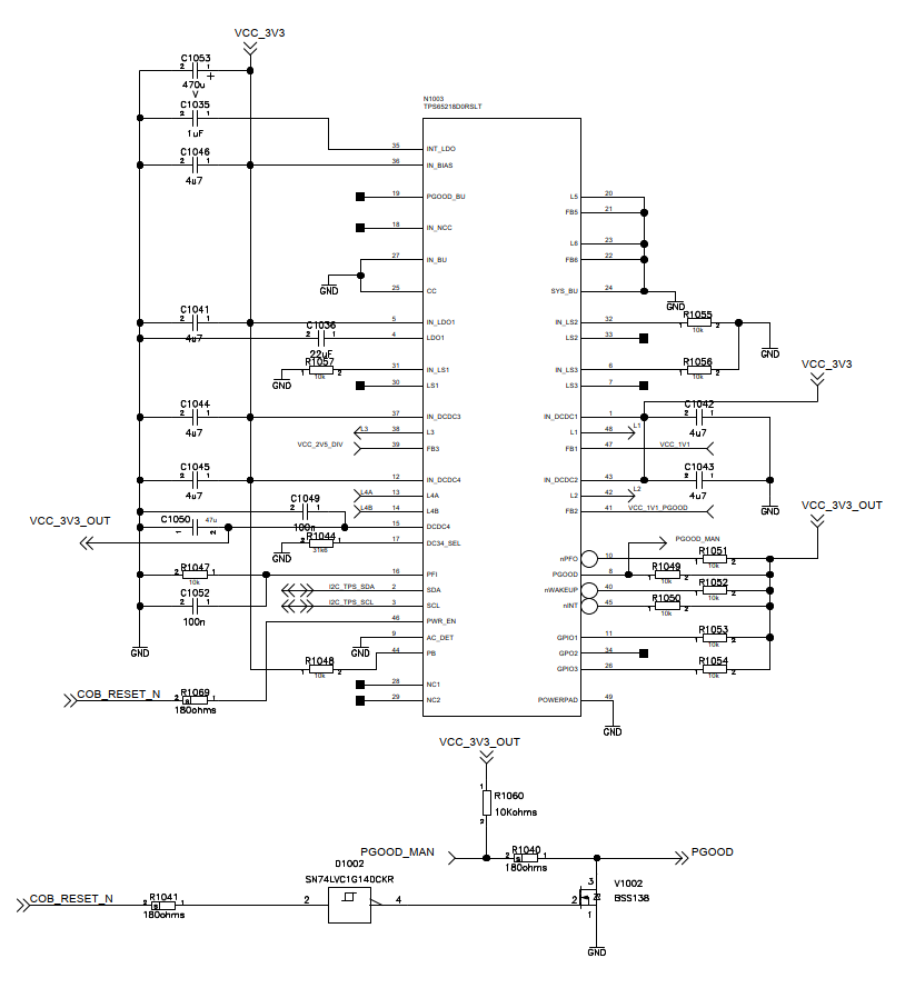
I'm using the TPS65218D0 to power a Cyclone V FPGA. The PGOOD output pin is connected to the nConfig Pin of the FPGA, to trigger a reconfiguration of the FPGA when the power is out-of-bounds. The TPS65218 is not reprogrammed using I2C, all the settings are as per default, meaning that also STRICT=1.
Unfortunately, when trying to configure a "larger" image onto the FPGA, one that using a decent amout of logic and I/O, a 400ms cycle of reconfigurations happen. The reason for this, that every time a new configuration tries to start, the PGOOD goes low for a duration of amout 1us.
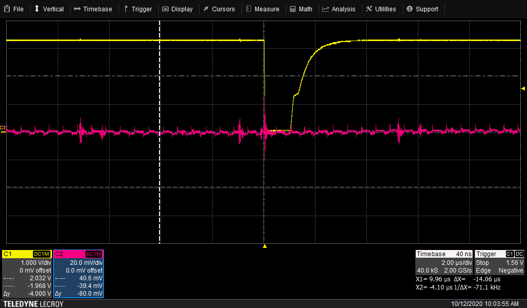
In the screenshot below, the yellow is the PGOOD signal, DC-coupled. The red signal is the output of the DCDC1, AC-coupled without a limitation of bandwidth.
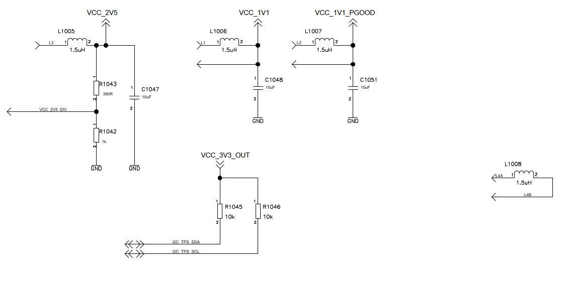
With measurements, I am not able to detect any change in voltage that should trigger the PGOOD signal, on either of the rails. The DCDC1 to DCDC3 have noise up to 20mV, DCDC4 has up to 40mV, which at a voltage of 3.3V should not be a problem, either.
And what confuses me too, how can it even be that the PGOOD is low for only 1us? Shouldn't the deglitch of the monitoring prevent this?
When starting the reconfiguration of a smaller image, or when using the DEV_CLRN pin of the FPGA instead of the nConfig, the system works without a problem.