This thread has been locked.

If you have a related question, please click the "Ask a related question" button in the top right corner. The newly created question will be automatically linked to this question.

BQ500212A: Circuit based on bq500212A bqTESLA Wireless Power TX EVM

Part Number: BQ500212A

Hello,

First of all, I know that this chip is not intended for new designs, but I have a big batch and I need to solve this (probably stupid and small) design issue, so please help. I am a student and it helps me learn.

I am building a charger for a small hand-held wireless device.

I have followed the EVM and printed a PCB. Unfortunately, after assembly, the chip does not seem to respond or even power on.

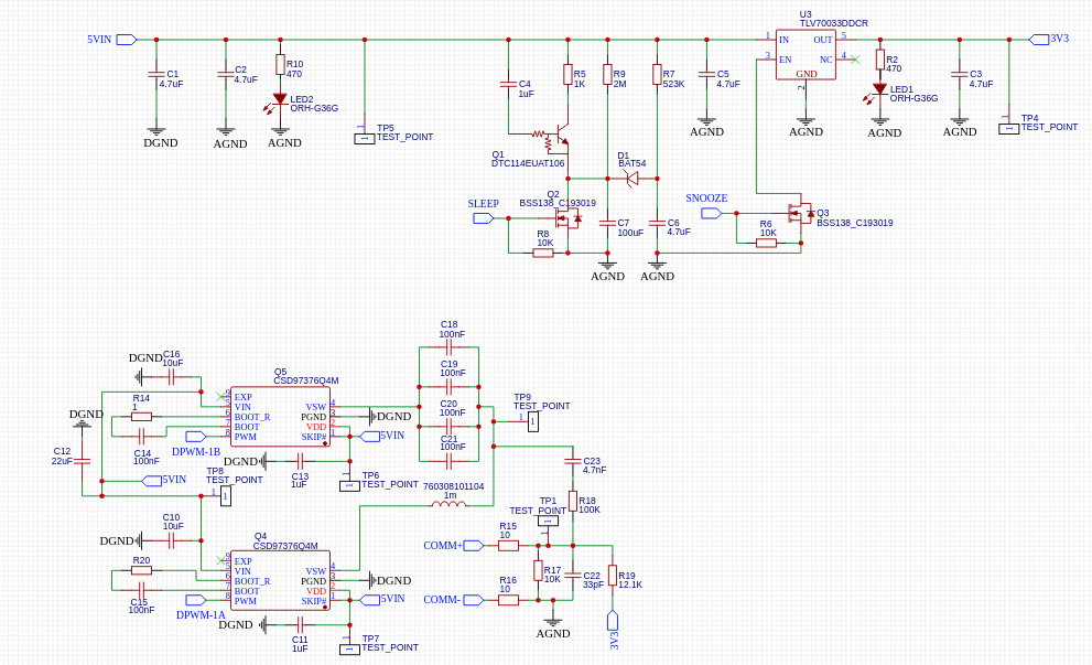
My schematic is here:
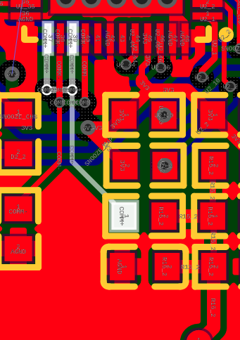
My layout is here

The first problem is that the 3v3 ldo never seems to come up, thus the chip never comes up.

The second problem is that even if I hardwire a 5V wire to the LDO EN, the chip still won't come up.

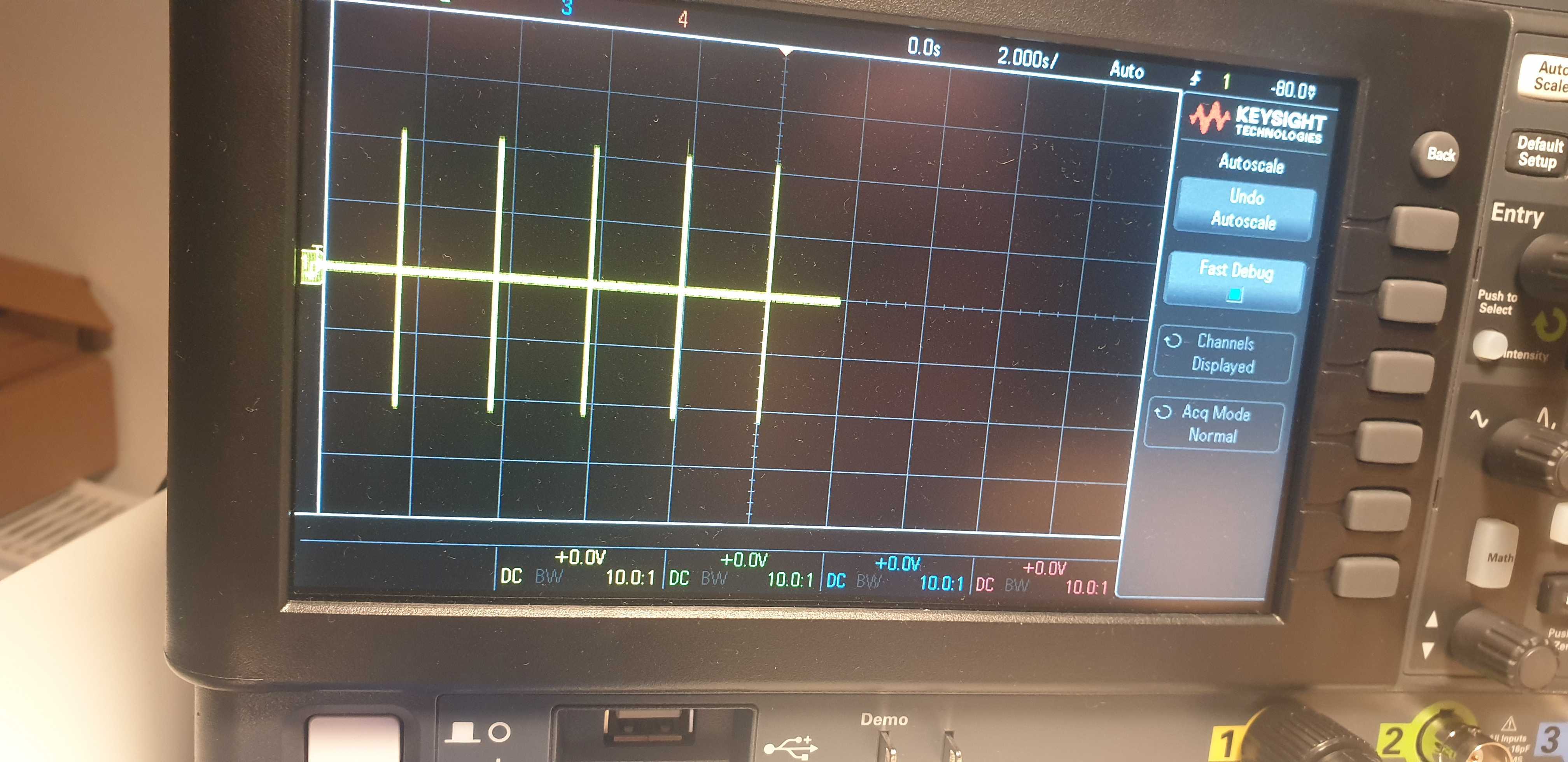
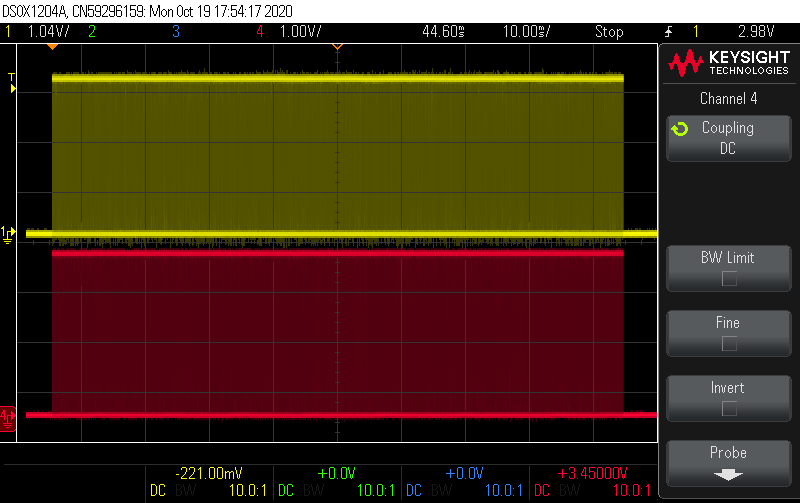
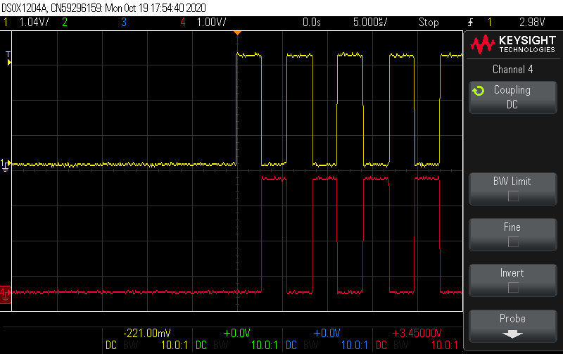
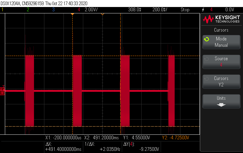
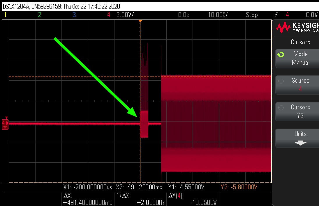
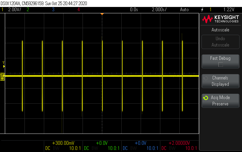
I have an oscilloscope and I tried to check every chip input and it resulted in this:

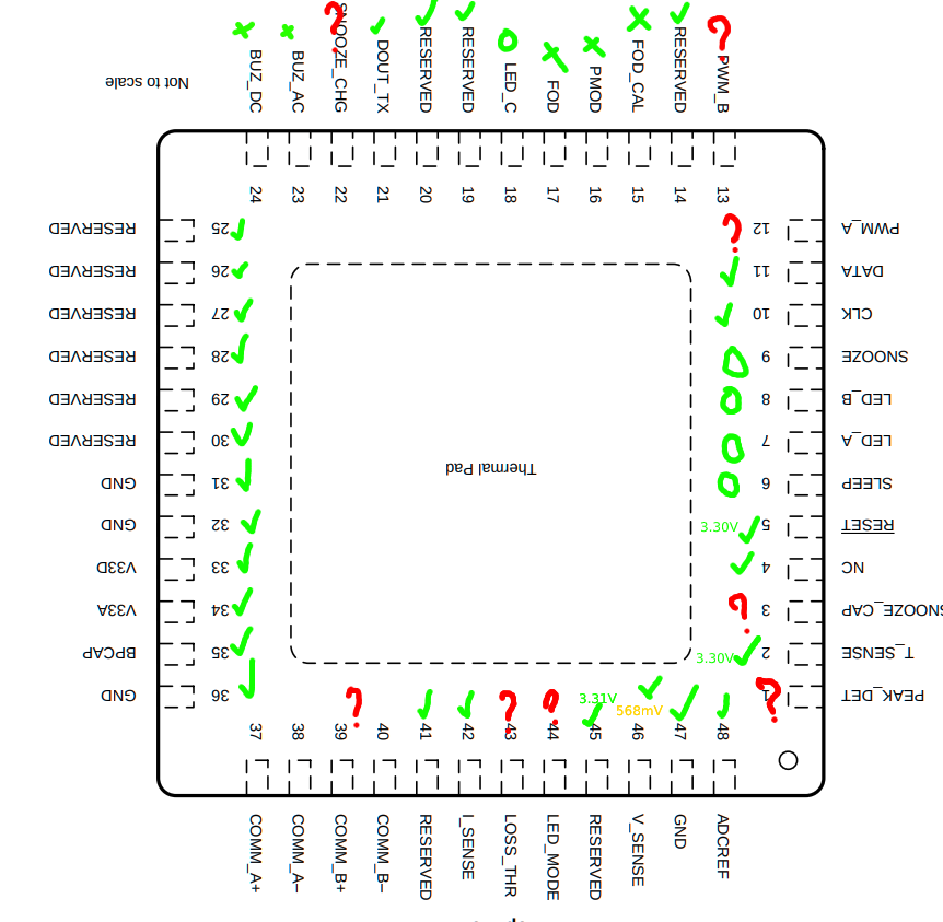
Note that PMOD, FMOD, T_SENSE and I_SENSE are not meant to be used for this.

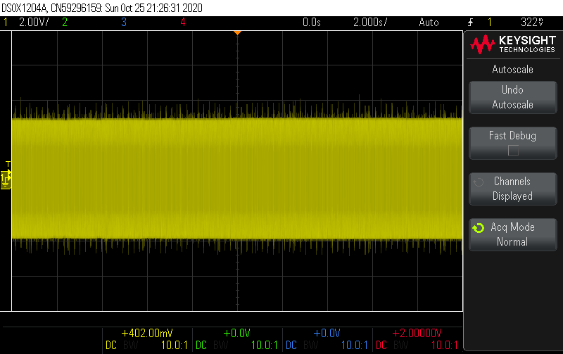
On top of this, I see not PWM output from PWM pins  or anything near the two half bridge mosfets.

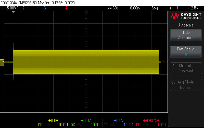
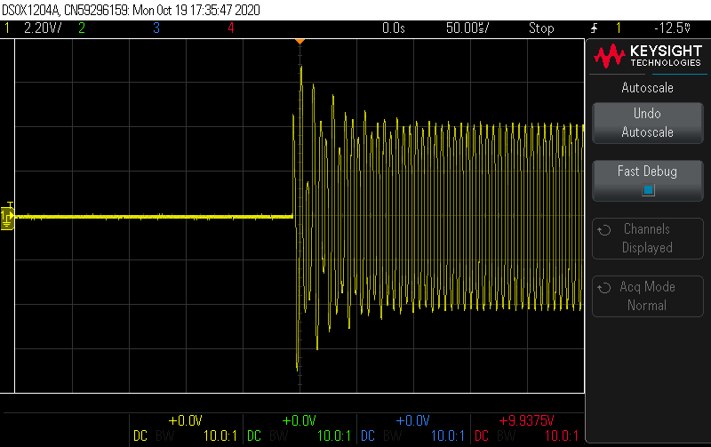
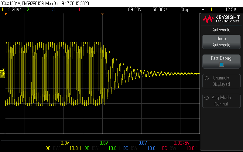
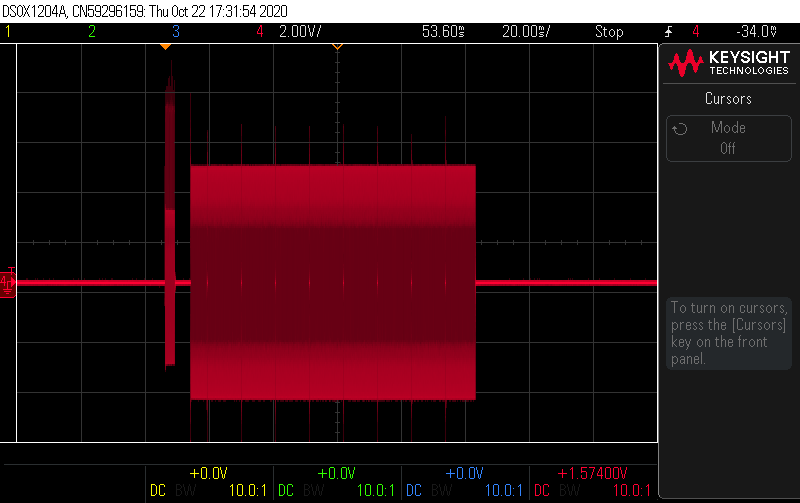
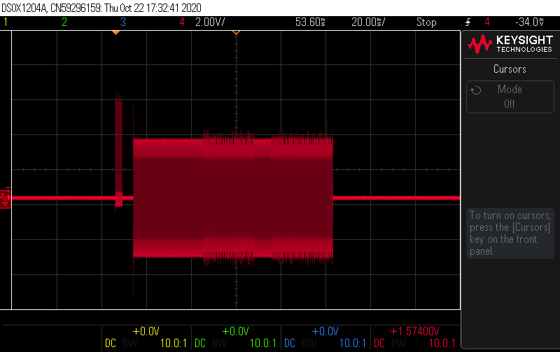
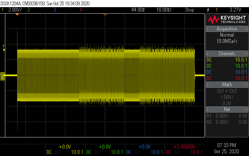
Finally, I tried to make sore this is not a soldering problem:

Here is a topic of discussion about this. In the meantime I assembled a secondary board to make sure.

Any thoughts?

Any help would be useful for learning

  • Hello

    Double check the connection to pin 35 of BQ500212A.  It looks like 3.3V is connected to the pin.

    This is 1.8V internal core voltage and should have capacitive divider connected to it, 1uF to gnd and 1uF to 3.3V.  A 2.2uF will work also.  Trying to get the core to power up before IO lines.

  • Thank you so much for your response. 

    I am in the process of rectifying this on the board.

    One question arises: When I will have divided the voltage, the voltage reaching the BPCAP pin will be 1.65V. I understand that I missed this divider from the original board, but there is no other mention of this voltage, except for this 

    This does not say how much voltage, nor do the next pages of the document inform about this. 

    How would one know what to use otherwise?

    Another question is: How is the LDO turning on (given that the LED_MODE resistor is not disabling the SLEEP/SNOOZE functionality: For example 75k ohm)? 

    It just does not click with me that it will turn on at any point without having the chip powered on first. Maybe I do not understand the underlying electronics behind it? 

    Can you clarify this for me? 

    Thank you very much!

  • I have managed to turn one board on.

    I get this kind of ping at the tx coil end, it also propagates to the receiving device:

    Unfortunately, I don't see anything on the COMM. What should I look for? I analyzed this document before.

    Any help would be useful

  • Hello

    The TX should send a digital ping every 500ms to check for RX, the RX will reply during this time and TX will keep power applied.  

    More info on this in the attached TX trouble shooting guide.

    5556.bqTESLA FAQ--TX Trouble Shooting Guide.pdf

  • Hello,

    I have followed the troubleshooting guide accordingly and I have the following problems:

    My pings are spaced out too far and I do not know how to read the RX protocol. 

    My pings happen every two seconds and they look like this:

    I understand that they are driven by the PWM signal, which looks like this

    What alters the timing of the PWM signal? In the datasheet, it says "The deadtimes must be externally generated". The only timing circuit on the board is the SNOOZE_CHG/SNOOZE_CAP. Any idea?

  • Hello

    What we should see is a some modulation on the coil voltage from the RX.  Take a look at the point when TX coil and Resonant capacitors connect
    (400nF).  You should seen the signal from RX at that point.

    Also to make test easier continue to test with LED MODE pin grounded this will disable the sleep mode. The sleep circuit can be debugged later.

  • Hi,

    Thank you for instructing me to disable LED_MODE and how to check for RX messages.

    Here's what I've found. Is this what I'm looking for?

    NO RX

    WITH RX

    After I disabled LED_MODE three things changed: First, the  time between pings is around 490ms

    Second, I see this ripple with every pulse:

    and finally, I hear this buzzing noise, almost like an arch inside one of the components.

    Any ideas?

  • Hello

    The below scope capture looks promising.

    We can see the reply from RX, ripple in the top and bottom.  This is the serial word, first is ok this is signal strength, 2ed word identification is sent but has a decoding problem and power transfer stops.

    The quality of the modulation is OK problem could be grounding on BQ400212A or issues with -COMM/+COMM circuit.

  • Hello

    The BUZZ --- hard to say, it could be noise from filter capacitors this is common. If you can get the unit into power transfer it will be easier to debug.

  • I have my COMM lines above. It might be the COMM lines.

    My comm lines show 0 V. 

    I read that the COMM+ should be centered @ 1V. How to? (See my above schematic/circuit)

    They look like this on the board:

    I could not find how they were connected in the EVM. This is what I did.

    One question: Is there some documentation on what the pulses from TX should mean? I believe there should be a well-established protocol, where can I find it?

    Also, thank you Bill for your support so far!

  • Hello

    I did not see anything in the layout or schematic that could cause problems. 

    Try adding a filter capacitor to the 3.3V going to R19 at COMM +/- circuit, about 100nF.  Ground for cap should be at the circuit, R17/C22 gnd.

    Comm +/- will sample the lower half of the LC tank circuit, divide it down and bias it to 1.5V before applying it to device for demodulation.  Noise and grounding issues in this circuit will cause demodulation problems.

  • I removed the short from LED_MODE. For reasons that I don't yet fully understand, the ping with TX looks a lot better (although not yet functional). With the LED_MODE not shorted, the delay between pings is 2000ms. I will come back when I will have solved the biasing problem near COMM+/- (currently pulled to GND for some reason)

  • I resolved the issue with bad comm biasing. Something was wrong with the resistors. I either soldered bad value components or I was shorting them somehow. Now I have clear 1.5V bias at COMM+. Did not add the said capacitor.

    Not sure what I see now. Is this charging?

    Coils without LOAD:

    COMM with TX:

  • Hello

    The lower waveform is power transfer the coil voltage is remaining on.  This will only happen if COMM is working correctly.

    The upper trace looks like digital ping with no RX present.

  • Hello,

    By now I completed a few charging cycles and the charger works. 

    I am willing to do some more learning on the process of determining efficiency and whether this would be a WPC compliant board. I know that WPC requires FOD and T_SENSE etc, but I mean from the EMI/noise point of view.

    Do you have any great resources for learning about these aspects?

    Again, I am looking for ways to determine if my board would be suitable for EMI standards.

    I am intending to build an additional charger on the same board (as in one board charges two separate devices) in the future. Do you have any suggestions on that?

    Thank you for your help so far!

  • Good to hear you are running charge cycles.

    Do not have any EMI application notes.  But a very common approach is to layout the PCB to the dimensions of coil so that it will fold under coil then it acts as a shield.