This thread has been locked.

If you have a related question, please click the "Ask a related question" button in the top right corner. The newly created question will be automatically linked to this question.

TPS54519: EN pin current spec

Part Number: TPS54519

Hi team,

Customer requests the current spec required for EN pin. 

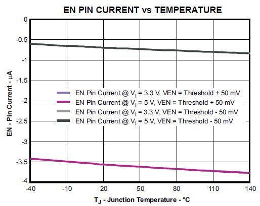
Unlike other devices that specify this spec in the table, TPS54519 does have a graph as below. Is it because this device has internally pull-up current source?

I'm confused with what this graph say, but in terms of the negative value in the graph, I believe that EN pin will 'source' (not 'consume') the current. And the gray line is saying that EN pin will source -0.5 to -1uA by internal current source if the pin pulling below 1.18V (threshold), and the purple line is saying that EN pin will source -3.5 to -4uA if the pin exceeding 1.18V. Could you correct it if any misunderstanding here?

Plus, customer basically requires this spec to estimate if the current consumption is met to the sequencer's possible sourcing current spec. If this device has a negative EN pin current, it will supply the current into the sequencer, right?

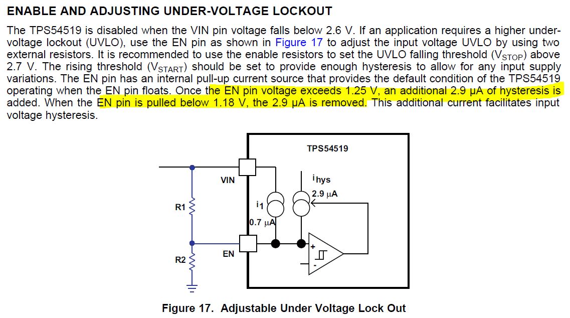
For your  information, they don't use this pin as UVLO. It's only connected with the enable signal from the sequencer.

Thanks,

  • Hello KIM,

    The case you can see detailed in the datasheet shows a resistive network R1/R2 where the current from the EN current generator will flow to the GND of R2.

    The current will then be negative because flowing out of the device from the input side. It then means that the EN current should flow towards the sequencer. 

    I would assume that the current would not flow towards the sequencer if the voltage applies at the EN is higher than the VIN. 

    Thanks,


    Dorian

  • Dorian,

    Please check the schematic below. Is it okay to directly drive EN without resistor dividing circuit to VIN? PWR_ENABLE_2ND is coming from the sequencer. So in conclusion,

    VEN = threshold-50mV (device OFF) --> 0.7uA will flow out of the device toward the sequencer

    VEN = threshold+50mV (device ON) --> 0.7uA plus additional current of 2.9uA would flow out of the device toward the sequencer

    If this assumption is correct, I just thought that this reverse current toward the sequencer may be able to cause harm on the sequencer, thereby affecting the EN operation. Could you tell me your opinion on this? Has any customer ever considered EN current in terms of the sequencer current spec?

  • Hello Kim,

    I also understand the EN operation to be working like you described.

    My assumption here is, that the current will be stored in the capacitor you connected to the EN pin. I would also look at the sequencer current specfication to make sure this is not a cause any issue.

    This is not a common circuitry for the EN operation in our portfolio, if this is a problem for your surrounding circuitry. I can recommend you the use of different part.

    Let me know if I can help!

    Thank you very much,

    Regards,
    Dorian   

  • Hello Kim,

    I haven't heard back from you.

    Do you have any further questions here?

    Please let me know!

    Regards,

    Dorian

  • Hi Dorian,

    From your assumption, I guess the current from the internal current source would flow into the capacitor at the very first time, but after it's fully charged, the current would still be sourced from the internal current source to the sequencer. Please correct me if you have any better idea..

    I informed customer of the expected sourcing current of 3.5mA when voltage H is applied. It's the all to do from our end, and board design is up to the customer!

  • Hello Kim,

    I also had the same understanding here.

    Did you get feedback from your customer, either or not it is something they can live with ?
    Thanks,


    Dorian

  • No, I haven't get any feedback from customer. I'll update here once I get it. Thank you for your kind help!