This thread has been locked.

If you have a related question, please click the "Ask a related question" button in the top right corner. The newly created question will be automatically linked to this question.

UCC28C43: No PWM output

Part Number: UCC28C43
Other Parts Discussed in Thread: UC2843

Dear TI Support team,

We are using UCC28C43 in a flyback design. The FB pin is connected to 0V and the COMP pin is controlled by opto-isolated feedback.

The design is for 200V DC input and 56V DC output.

To begin with, I have started testing at lower input DC voltages to check functionality. I am testing with about 70V DC input by reducing the start up resistor to 10k Ohm.

The VCC pin rises above UVLO turn ON threshold at about 40V input and we get VREF output of 5V. At 70V DC, the VCC is about 13V.  Saw tooth waveform is generated at RT/CT pins. Part of the saw tooth waveform is added to ISENSE pin through a transistor (similar to that shown in Fig. 27 of the datasheet). The peak ISENSE pin voltage is about 0.6V. Currently there is no opto-isolated feedback (as it will get activated when the output gets close to 56V). COMP pin is at around 6.3V.

Under these conditions, there is no PWM output. The voltage at ISENSE pin is solely the result of the saw tooth waveform added there.

As per my understanding, if the COMP pin is at 6.3V and ISENSE pin peak voltage is 0.6V, I should get close to 100% PWM duty cycle. But actually the output continuously LOW.

I tested with the above arrangement on 3 boards, with the same result.

With regards,

Vijay Limaye

Request your support for resolution of the problem.

  • Hi,

    If the PWM comparator output is latched LOW, R=0 and R never sees any edge (RS flip flop is edge triggered), OUT is latched LOW. As an experiment, try increasing CS by increasing your slope comp and/or pulling COMP to within the range of 2~3V...really you need your opto providing feedback to COMP since you have FB connected GND.

    Steve M

  • Hi,

    Thank you for your reply.

    I tried the experiment as per your suggestion by increasing slope compensation so that ISENSE pin crosses 1V threshold during each clock cycle. However, there is still no PWM output, it is still LOW.

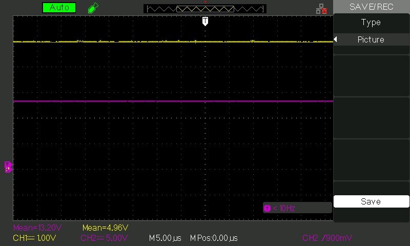
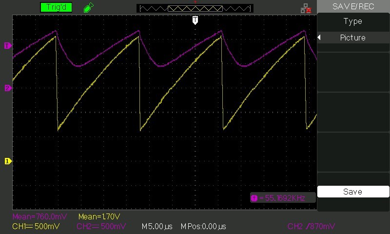
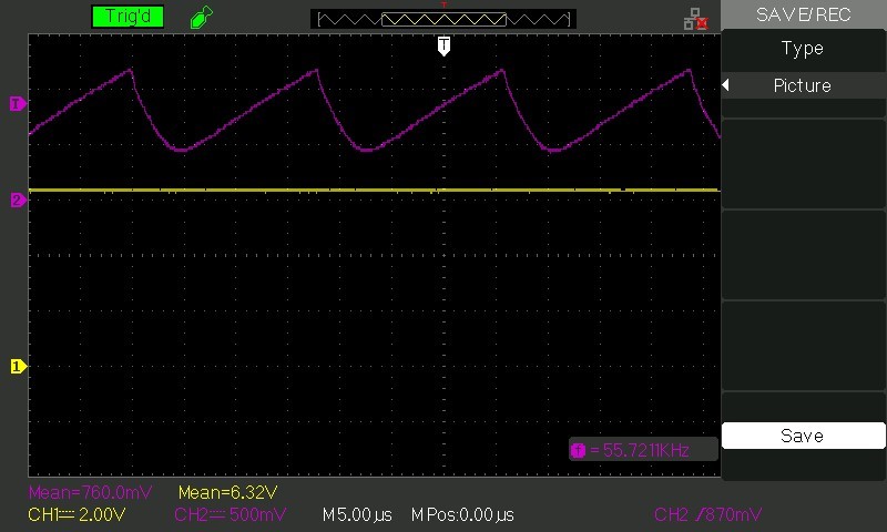
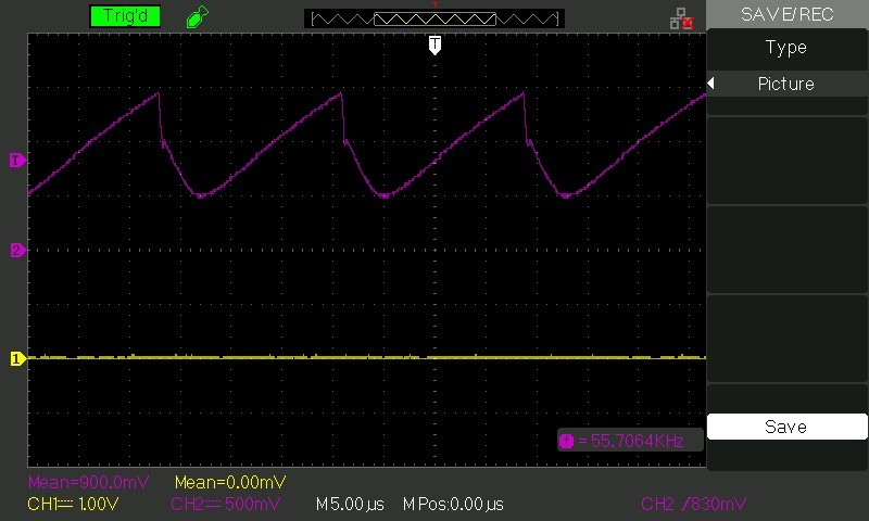
    Please see below some waveforms (may be helpful for analysis). I only have a 2-channel oscilloscope, so I could capture only 2 waveforms at a time. All the waveforms are under same operating conditions.

    CH1: VREF   CH2:VDD

    CH1: RT/CT CH2:ISENSE

    CH1: COMP CH2:ISENSE

    CH1: OUT CH2:ISENSE

  • CH1: VREF CH2:VDD

    CH1: RT/CT CH2:ISENSE

    CH1: COMP CH2:ISENSE

    CH1: OUT CH2:ISENSE

  • Can you please share your schematic or even a hand drawing of what components are on the UCC28C43 pins?

    Regards,

    Steve M

  • Please see below the schematic for your reference:

    One opto-coupler is for feedback and the other is to Enable/Disable the converter.

    Regards,

    Vijay

  • The schematic shows UC2843, the actual part used on board is UCC28C43D.

    With regards,

    Vijay

  • Vijay,

    Please try reducing the impedance see at the CS pin. Please make the following changes:

    1. R3: 1k--->100
    2. R5: 1.82k ---> 182
    3. C9: 470pF--->4.7nF

    This maintains the same scaling as your original design but your RC filter on CS still seems large to me. You have a corner frequency of ~340 kHz and your switching frequency is ~55 kHz. You are losing some linearity in your CS signal - consider RC filter corner frequency at least 10x the switching frequency and possibly as high as you can allow while maintaining effective CS filtering.

    Steve M

  • Hello Steve,
    Thank you for your reply. I will optimize the RC filter as per your suggestion. However, the original problem (no PWM output) remains unresolved. I tried by changing component values (R3 -> 100, R5 -> 182, C9 -> 4.7nF).
    With these changes, the ISENSE pin waveform does not cross 1V peak. So, I restored R3 to 1k and C9 to 470pF. Now the ISENSE pin peak reaches about 1.7V. But still there is no PWM output. Please see below the waveforms for RT/CT and ISENSE pins.

    With regards,

    Vijay

    CH1: RT/CT   CH2: ISENSE

  • If the CS pin had a certain peak before you made the scaled down component changes I recommended, the same peak should be attained (neglecting the small value of the CS resistor). all components are scaled correctly and the CS peak moves as a result, then some other impedance seen at the CWS pin must be present. How about scaling down RT, CT? If you reduce RT to the minimum recommended value you can use for the frequency your are trying to set, you will have additional current  available. If all these recommended changes still produce no output, you may have a PCB/component issue?

    Steve M