This thread has been locked.

If you have a related question, please click the "Ask a related question" button in the top right corner. The newly created question will be automatically linked to this question.

UCC21732-Q1: Active miller clamp effect simulation

Part Number: UCC21732-Q1
Other Parts Discussed in Thread: UCC21732

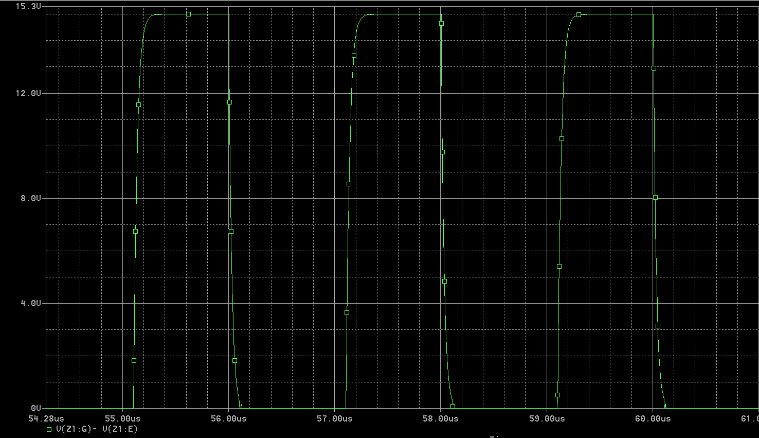
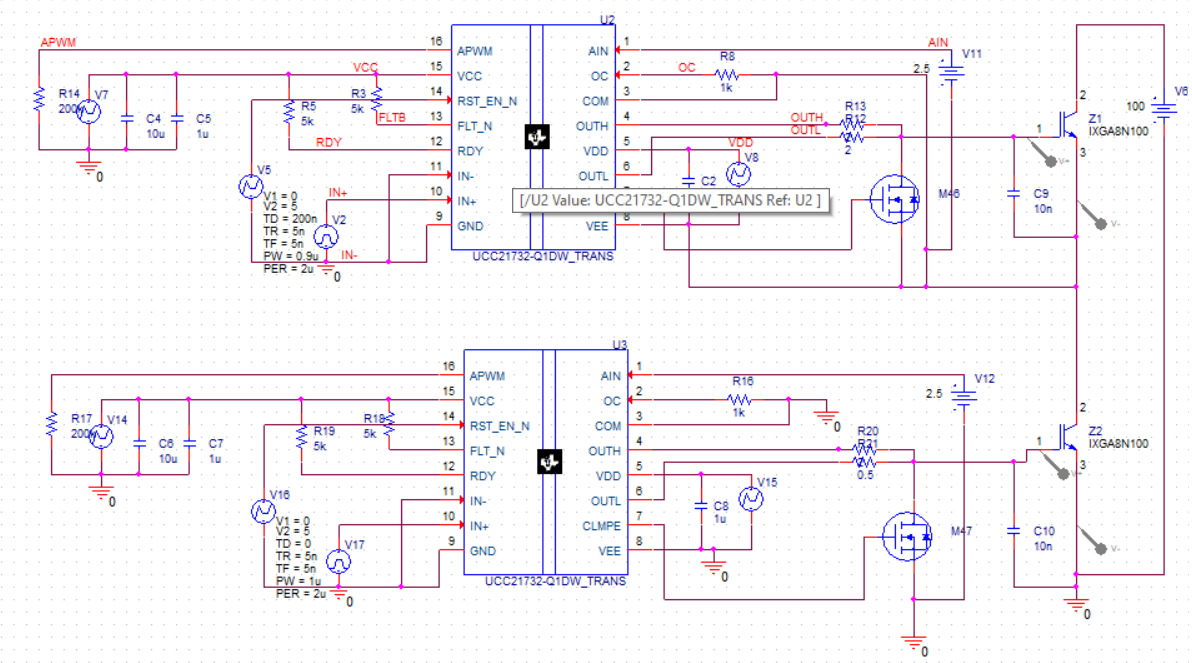
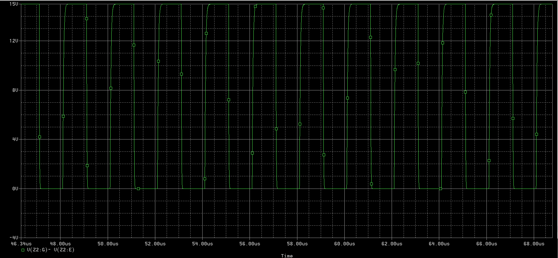
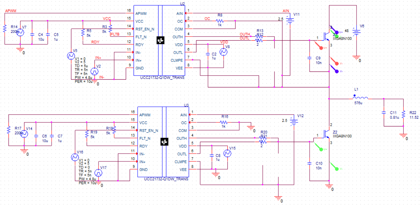
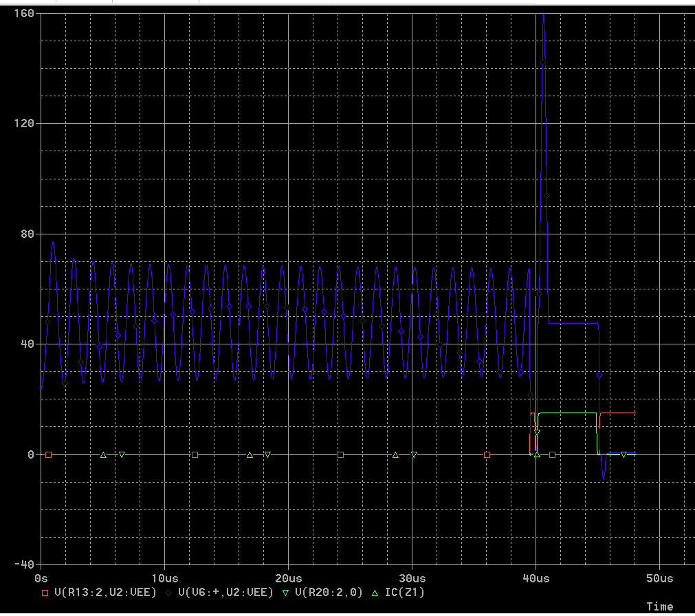
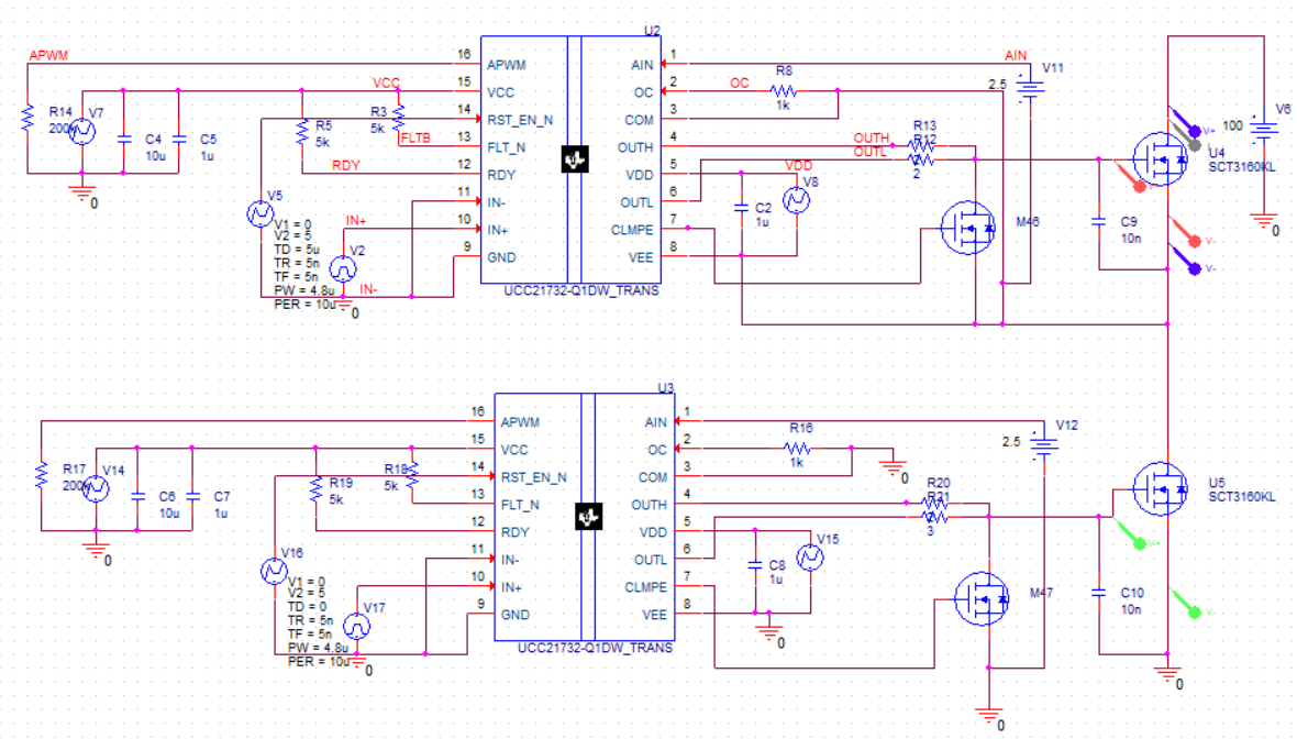
I am trying to study the effects of dv/dt on SiC MOSFET false turn-on. I am using UCC21732 gate driver IC from TI. Initially I am simulating using the downloaded files from TI website, which has an IGBT in place of MOSFET. My problem is that when I simulate it for DC Bus voltage = 100 V at switching frequency on 500kHz, (a higher DC bus like 500 V does not converge in Pspice sim) I am getting a few millivolts glitch in the top device, but no glitch at all in the lower device. This is happening for both with active clamp MOSFET and without it. I tried to go from 10V to 50V to 100V but I don't get anything with any value of OUTH and OUTL resistors for the lower device. Here is my circuit and waveform:-

  • Hi Shalini,
    Thanks for reaching out to E2E!  That does seem to be odd...  my colleague will get back to you on Monday to work on this with you.

    Thanks,

    Aaron Grgurich

  • Hi Shalini,

    In the schematic there's a couple things that we could try.

    • Could you add an inductive load to the switching node to see the effect on the gate of the IGBT's
    • In order to see the dv/dt effects disconnect the CLAMP MOSFET as this MOSFET will mitigate the effects
    • Increasing R21 will also allow to see the effects of dv/dt better

    Could you please share the results with the changes mentioned above.

    Let me know if there's any questions.

    Best regards,

    Andy Robles

  • Hello Andy,

    I tried out a few of the suggestions. Earlier I did try both with the Clamp as well as without. Here are my new results:-

    1) I cannot seem to add an Inductive load. I made calculations in a similar method to a synchronous buck chopper, but it is giving me wrong results or just getting stuck in 49% simulation. The error does not seem to pertain to Simulation Settings. I think it is because of large L1. So I tried different values, but it's always giving me wrong answers. Please suggest an inductive load to be added. I have attached the circuit with the large L1 value.

    2) Without the inductive load at the switching node, I tried with both the IGBT and the SiC MOSFET, and there seems to be some improvement, although the glitch is not as high as I want it to be simulated at. My results are something like this:-

        IGBT :  100kHz, all Rg = 2 Ohms, DC Bus = 100V : Upper device glitch = 387.4mV, Lower device glitch = 352 mV [No clamp]

        MOSFET : 100kHz, all Rg = 2 Ohms,DC Bus = 100V : Upper glitch = 332.1mV, Lower glitch = 318 mV [No clamp]

                                                                                             : Upper glitch = 51.88mV, Lower glitch = 50.1 mV [Clamp]

                           100 kHz, lower device Rg_off = 3 ohms , DC Bus = 100V: Upper glitch = 48.43 mV   [With Clamp]

    My problem in this point is that I cannot increase the DC bus more than 100V because it is not converging in Pspice. Nor can I change the Rg-off to 0.5 ohms. I want to vary the external gate resistances and bus voltages, and switching frequency to study the miller clamp effects. 

    Here are the images corresponding to Point 1:-

    Here is the circuit that is corresponding to point-2

  • Hi Shalini,

    For an inductive load could you try connecting the inductor alone from the switching node to GND.

    I will be running some simulations under the conditions shown in your schematic, but will need some time to get to this. I could get back to you early next week. Would that be okay? 

    Could you email me to continue this conversation.

    Best regards,

    Andy Robles