This thread has been locked.

If you have a related question, please click the "Ask a related question" button in the top right corner. The newly created question will be automatically linked to this question.

UCC21222: half bridge Gate driver layout

Part Number: UCC21222

Hi 

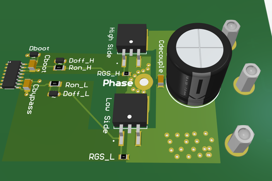
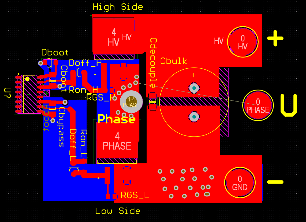
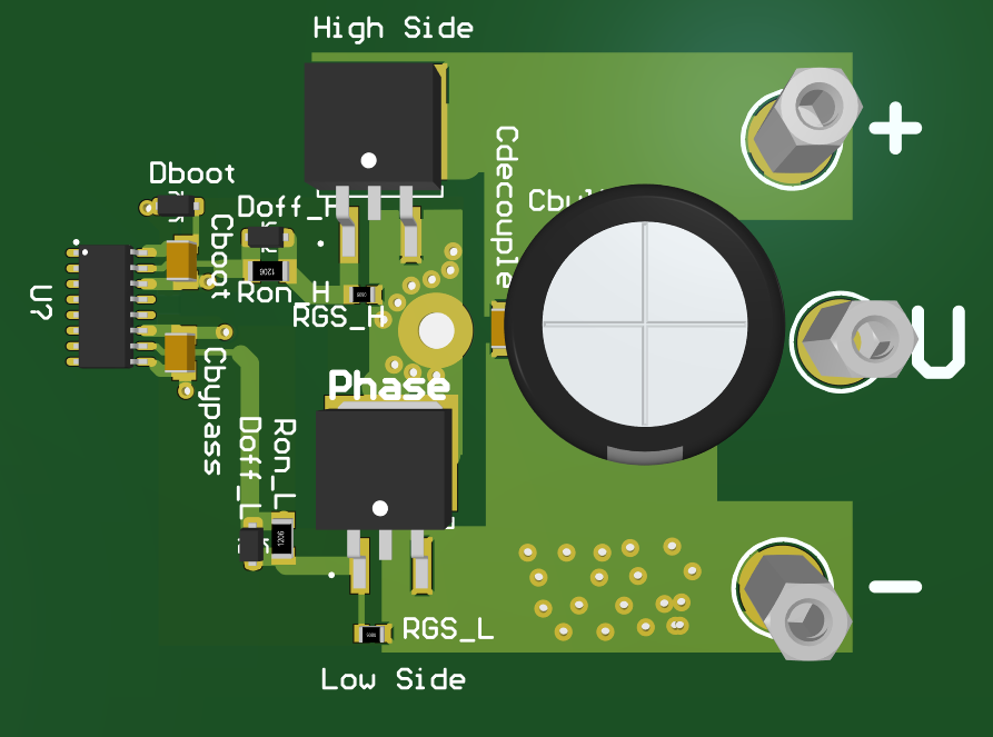
I am trying to design a half bridge for motor driver 36v-48v , based on what i read in several appnotes like " Best Practices for Board Layout of Motor Drivers".

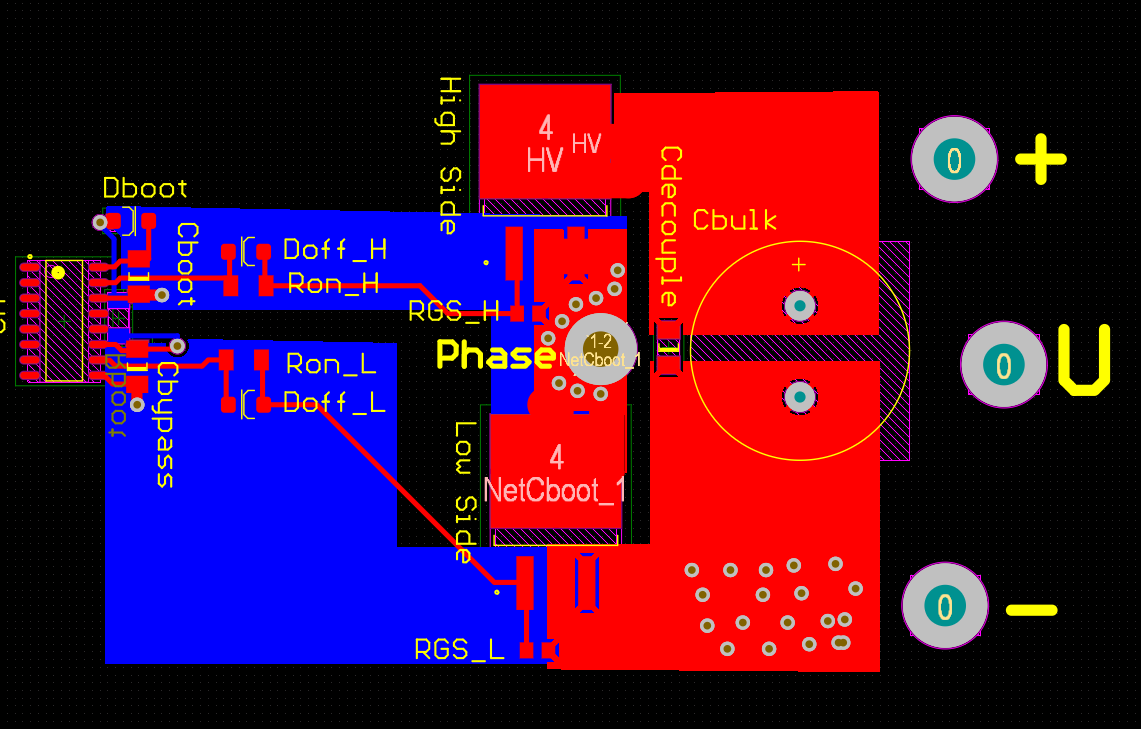
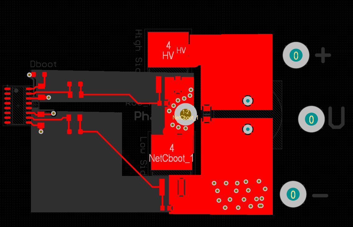
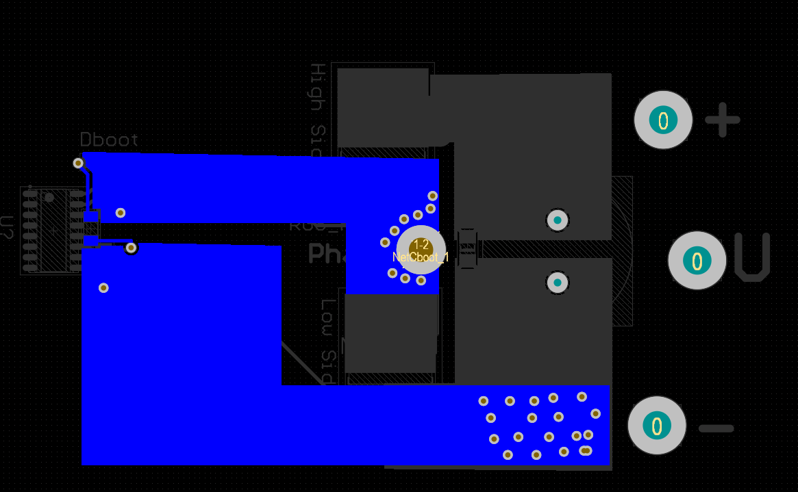
I have drawn this simple circuit and i want to know if the layout applies the rules to minimize inductance and reduce switch node ringing:

1. Each gate signal has the the return path (reference plane) under neath in the bottom layer.

2. switch node (denoted here as phase) doesn't cross the power HV and GND planes and doesnot come close to Low side gate signals. 

Question : Which is better , using a wire to connect point Phase to the standoff "U" externally , or using a 4-layer board and connecting these 2 points using internal plane ? 

Any other suggestion regarding making the layout better? 

note: this is an example only to grasp the idea, the real circuit will have 3 mosfets in parallel , and it will be more tight ( the gate driver will be closer to the mosfets)

  • Hi Bob,

    Thanks for reaching out to E2E!

    Regarding your main question, I will have my colleague help you once they are back in the office on Monday.

    Regarding other suggestions; I have a couple you are probably already aware of as you said, the trace lengths, component placement distances, etc.  Also consider increasing trace widths, even via distribution, and component orientation to reduce gate trace length and current loops.

    Thanks,

    Aaron Grgurich

  • Hello,

    I may address the PCB layout based on the image you shared.

    The first priority when completing a PCB layout is the gate drive loop from VDD capacitors, to driver output stage to gate connections to ground return. You want to ensure that this loop is as small as possible to limit parasitic stray inductance in the gate drive loop which will limit peak current path and compromise gate signals. From your picture, driver connects to gate through long thin traces. You want to the gate traces as wide as possible and as short as possible.

    Because of the expected dv/dt on switch node (high-side source_low-side drain), you want to confine this signal to a minimal area with appropriate thermal considerations and appropriate distance from LO signal.

    I suggest you review section 12 of the datasheet as a starting point then let us know if you have additional questions.

    Regards,

    -Mamadou

  • hello,

    your points have been taken into consideration: now the gate driver is closer and the traces are 3 times as thick.  please check the Images attached and tell me what do you think . and 

    I have several points that need clarification: 

    1. you said the switch node should be confined to a minimal area . Does this mean what i made  is wrong ? ( I extended the switch node into buttom layer under the upper mosfet gate signals thinking that in this way i am making the loop as small as possible by running signals over their reference plane)

    2. You didnot comment about the question i asked regarding : using 4 layer vs using external wire to connection "phase" to "U". 

  • Hello,

    1. There is no wrong answer, it is matter of optimizing the performance of the ICs and minimizing risks of failure for the driver and FETs. Your design may work without failure but you might not be getting the best performance out of the bridge. I suggest you bring the FETs closer to each other and closer to the driver IC and rotate High-side FET 90deg clockwise. You may also consider rotating low-side FET (90deg clockwise depending on your application creepage and clearance requirements).

    2. You may connect externally through the bottom layer so long as no digital or low voltage traces nearby which from the looks of it, is not the case. 

    Regards,

    -Mamadou