

About schematic and layout for TPS6590378, I have question about SMPS1_2_FDBK_GND and SMPS4_5_FDBK_GND pin setting.
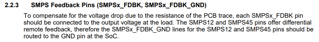
Application note: TPS659037 Design Guide is described below;

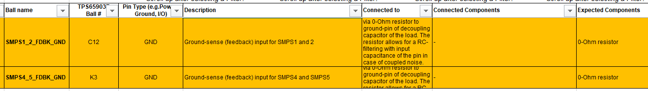
But TPS659037 Design Check List is described below;

I think that layout can not compatible with below two information, because it is difficult to implement by also the influence of TPS6590378 pin assign.
(When implement, I guess these layout should make long wire length and large loop area)
【Question】
・Which information is correct? (0Ω resistor area is require or not)
・Is 0Ω resister strongly recommend?
・When possible to implement layout for compatible with two information, please let me know reference design or reference layout.
Best regards,
Satoshi
