This thread has been locked.

If you have a related question, please click the "Ask a related question" button in the top right corner. The newly created question will be automatically linked to this question.

BQ25713: BQ25713 En_OtG bit autoclearing whenever OtG operation is attempted.

Part Number: BQ25713
Other Parts Discussed in Thread: TPS65987D, , BQSTUDIO, TPS65987

I'm having an issue in which the En_OtG (bit #4 of Reg. 0x35) clears upon the instant that I make the OtG/VAP pin (#5) high, and as long as such pin is high, I can't set such bit high again and thus can't activate OtG. Of course, I also have the OtG_VAP_Mode (bit #5 of Reg. 0x34) high and appropriately set the OtG Voltage Register to 5.009V and the OtG Current register to 500mA. I normally use the Low OtG voltage range (bit #2 of Reg. 0x34 High)

Such issue is driving me nuts.

Could you please enumerate all the conditions on which such En_OtG bit will be cleared when OtG operation is attempted?

I know of some possibilities:

1) OtG_OVP & OtG_UVP (bits [1:0] of Reg. 0x20). I know definitively that there's no OVP as the adapter side doesn't rise at all, but I don't know about UVP. At what point upon enabling OtG is a UV condition declared? Does it start switching for a few milliseconds and if it hasn't risen to a given point it quits and disables En_OtG? I can't see any switching attempt nor battery current draw burst when I set the OtG pin high.

2) I know that the battery voltage cannot exceed the the Charge Voltage Register by more than 2% so that there be no Battery OVP condition which would inhibit OtG operation. I set the Charge Voltage Register to 8.856V yet I have the battery voltage at 8.2V so there's no risk of OVP tripping whatsoever.

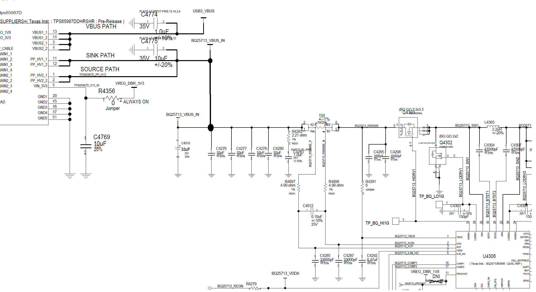
3) I have ILim_HiZ being driven to 1.2V (for initial 500mA limiting) via a 175.1KΩ(Top)/100KΩ(Bot) divider powered from the TPS65987D's LDO_3V3 output. I confirmed I indeed have 1.2V.

Again, please kindly provide me with all the conditions that may cause the En_OtG bit to autoclear so I may troubleshoot accordingly.

Most Grateful,

Georg A. Mussenden

  • Also forgot to ask...

    On page 21 of the BQ25713 spec. it's stated that "The OTG output voltage transition slew rate can be configurable, which is complied with the USB PD 3.0 PPS specifications".  Where's the register for such configuration?  Could it be that it's inadvertently set to all zero thus not allowing the OtG output to rise?

    Thanks so much!

    Georg A. Mussenden

  • Hi Georg,

       The output of OTG mode is on VBUS. Do you have an adapter present while you are trying to enable OTG?

  •  No adapter, what's plugged-in is a little jig board that plugs into our product's Type-C receptacle which presents an Rd (5.1KΩ) into one of the CC lines which then causes the TPS65987D to drive High its GPIO1 which connects to the BQ25713 OtG/VAP line.

    What's really important for me to understand at this moment is what set of conditions cause the En_Otg bit to autoclear..

    This is how the two chips interconnect at a VBus level:

  • Hi Georg,

       The below conditions need to be satisfied first:

    • Valid battery voltage is set REG0x15(), the battery voltage should not trip the BATOVP threshold, otherwise, the converter will stop switching. •
    • OTG output voltage is set in REG0x3B() and REG0x32[2], if REG0x32[2] = 0, the VOTG digital DAC is offset by 1.28V to achieve higher range from 4.28V~20.8V, if REG0x32[2] = 1, the VOTG digital DAC is from 3V to 19.52V. •
    • OTG output current is set in REG0x3C().
    • The actual EN_OTG pin is high

    You want to verify that there are no fault conditions as well. An OTG UVP can occur if the load on VBUS is higher than the OTG Limit setting, causing VBUS to drop below the OTG_UVP setting, which is set as 85% of your OTG output voltage setting. Reading the status of the Charge Status register will indicate if any fault conditions is interrupting OTG.

    Also verify that your watchdog timer is not resetting any values back to its POR value, as default is OTG disabled.

  • Thanks Kedar, but it's not those obvious issues that are documented in the spec., it's something more taciturn.  One thing that I noticed is that we are [improperly] doing continuous writes to the Charge Voltage (0x04~0x05 )register whilst in attempted OtG.  Maybe the BATOVP state machine kills the OtG thinking that a Bat OVP condition could ensue as a result of such write activity - albeit such write value isn't below the Max. battery voltage.  I've asked our SW guy to remove such writes.  I'll let you know the results.

    Meanwhile if you can tally a list of taciturn items that can dislodge OtG please kindly do so.

    Most Grateful,

    Georg A, Mussenden

  • Hi Kedar!  Our SW guy eliminated the spurious writes to the Charge Voltage Register, but that didn't fix the issue..

    One thing that I seem to see is that Register 20's bit #0 (Fault_OtG UVP) seems to get set and that disables OtG.  I can't see any attempts on Q4 to switch.  Q4 works fine in normal forward mode as I can generate a 9V VSys from a 5V VBus which require Q4 and Q4 to switch as to boost.from 5V to 9V.  During OtG attempted operation, I confirmed that Q4 has proper battery voltage on its Drain.

    Is there a description of how long the BQ25713 attempts to run before it declares an OtG UVP condition?  Also, are there any conditions (other than those discussed previously) that would inhibit the BQ25713 to switch its FETs in OtG mode?

    Thanks so much,

    Georg A. Mussenden

  • Hi Georg,

        What is your OTG current limit, and is VBUS loaded or unloaded while enabling OTG, and observing this OTG_UVP?

  • Is in the example below set to 1.8A and there's no load, the BQ25713 is connected to the TPS65987D as shown on the picture I posted above on October 21st.  The TPS65987D appropriately drives High GPIO0 which drives the OtG whenever it detects an Rd pulldown on one of its CC lines.

    It must be noted that the BQ25713 doesn't do an attempt to drive in switching manner the gate of Q4 (remember this is a reverse buck from 8~9V to 5V).  So it's not that it's trying to switch and then faces a heavy load/short and then collapse.  It simply refuses to switch and then declares a UV as obviously nothing comes out.

    Perhaps the commands I send can be of help to you to see if I'm doing something wrong:

    i2c wr8 1 0x6B 0x00 0x4E
    i2c wr8 1 0x6B 0x01 0x03

    i2c wr8 1 0x6B 0x02 0x00
    i2c wr8 1 0x6B 0x03 0x04

    i2c wr8 1 0x6B 0x04 0x38
    i2c wr8 1 0x6B 0x05 0x21

    i2c wr8 1 0x6B 0x06 0x9C
    i2c wr8 1 0x6B 0x07 0x09

    i2c wr8 1 0x6B 0x08 0x00
    i2c wr8 1 0x6B 0x09 0x24

    i2c wr8 1 0x6B 0x0A 0xC0
    i2c wr8 1 0x6B 0x0B 0x03

    i2c wr8 1 0x6B 0x0C 0x00
    i2c wr8 1 0x6B 0x0D 0x18

    i2c wr8 1 0x6B 0x0E 0x00
    i2c wr8 1 0x6B 0x0F 0x3C

    i2c wr8 1 0x6B 0x30 0x00
    i2c wr8 1 0x6B 0x31 0x92

    i2c wr8 1 0x6B 0x32 0x7A
    i2c wr8 1 0x6B 0x33 0x00

    i2c wr8 1 0x6B 0x34 0x2C
    i2c wr8 1 0x6B 0x35 0x10

    i2c wr8 1 0x6B 0x36 0x64
    i2c wr8 1 0x6B 0x37 0x22

    i2c wr8 1 0x6B 0x38 0x00
    i2c wr8 1 0x6B 0x39 0x00

    i2c wr8 1 0x6B 0x3A 0xFF
    i2c wr8 1 0x6B 0x3B 0xE0

    Also I did read the Status Registers.  I entered everything in BQStudio so that it's convenient for you to use and analyze:

    * Created: Wed Nov 04 14:55:00 EST 2020
    *
    * Format: Register Name tab Character,\t Hexadecimal register value.
    * Device: bq25713
    * BQZ Container: Charger_1_00-bq25713.bqz
    *
    Charge Option 0 034E
    Charge Current Register 0400
    Charge Voltage Register 2138
    OTG Voltage Register 099C
    OTG Current Register 2400
    Input Voltage Register 03C0
    Minimum System Voltage 1800
    Input Current Register 3C00
    Charge Status Register 0000
    Prochot Status Register 8801
    Input Current Limit In Use 3C00
    VBUS and PSYS Voltage Read Back 0000
    Charge and Discharge Current Read Back 0000
    Input Current and CMPIN Voltage Read Back 00FF
    System and Battery Voltage Read Back 5555
    Manufacture ID and Device ID Read Back 0040
    Device ID Read Back 0088
    Charge Option 1 9200
    Charge Option 2 007A
    Charge Option 3 102C
    Prochot Option 0 2264
    Prochot Option 1 0000
    ADC Option E0FF

    Perhaps you can send me an equivalent set of commands that you guarantee will work.  Again, this is a 2S battery system.

    Most Grateful,

    Georg A. Mussenden

  • Hi Georg,

        What is the contract that the sink has negotiated? How are you sequencing the PD controller negotiating the contract and setting the OTG enable? I have not seen this issue before as PD+buck boost charger designs haven't run into this issue as far as I know.

  • Hi Kedar!


    The '65987D correctly drives the '25713 OtG line high (3.3V) when an Rd is present at its Type-C receptacle and low when it isn't.


    When facing a basic Type-C sink we present a [Legacy] 80µA Source Ip and we set the OtG current limit to something slightly greater than 1A. When facing PD sinks we offer a single 5V, 1A source PDO, again setting the OtG current limit to something slightly greater than 1A.


    Again, the primary question is why when the '25713's OtG line is High, whenever I try to set Reg. 0x35 bit 4 (En_OtG) High, it's immediately autocleared and a Reg. 0x20 bit 0 (OtG UVP) reported.
    As I asked, please examine the register contents I sent you to see if there's anything wrong and also please send me register contents that work for you.


    Thanks so much,


    Georg A. Mussenden

  • Hi Georg,

       I don't see anything that stands out from the register file. Do you have any updates from further tests tried?

  • Hi Kedar!

    I did some I2C tracing last week and Monday & Tuesday of this week and did find some mild irregularities like the OtG Volt/Curr registers being needlessly re-programmed quickly after entry into OtG mode which I had our SW guy remove and only keep the initial setting of 5V/1A, but that didn't fix matters.

    On Monday 11/23 I'll do power cycles whist inspecting with the scope the ILim_HiZ and OtG/VAP lines and see if ever (due to perhaps a TPS65987 glitch during initialization) the OtG/VAP line is High with ILim_HiZ being Low. I learned [the hard way] about 1½ years ago that if the OtG/VAP line is ever High with ILim_HiZ being Low, the BQ25713 won't ever re-enter OtG (with ILim_HiZ now at a proper Hi voltage which for our design is 1.2V) unless power is removed from the VBatt side (with of course no VBus source attached). I never could figure-out how to escape from such condition by means of register toying. Do you know how to clear such situation via registers? Such is a rather serious quirk as the product is with sealed battery so it's thus generally impossible to remove power and clear such event when the product actually ships.

    Please see the attached Pwr_I2C_StartUp_11_17_20_SW_TI.xlsx and Pwr_I2C_UponRD_Insertion_11_17_20_SW_TI.xlsx which respectively show the BQ25713 initialization and the programming that subsequently happens when a plug with Rd is inserted in our Type-C receptacle. On the latter, note in line 364 is where we become aware that the BQ25713 indeed entered OtG mode and on lines 447 & 448 where we become aware that OtG went UV and disengaged itself.

    Thanks so much and have a Great WeekEnd!

    GeorgPwr_I2C_StartUp_11_17_20_SW_TI.xlsx

    Pwr_I2C_UponRD_Insertion_11_17_20_SW_TI.xlsx

  • Hi Kedar!

    The issue I found out was that IDChg_VTh (Bits [7..2] of Reg 0x39 must not be zero (as it was in our SW), but rather the Max. continuous current that's expected to be drawn from the battery..

    Admittedly I didn't ever play with IDChg_VTh which the BQ25713 defaults to 0x20 (16.384A) but was somehow inadvertently changed to all zeroes in our SW.  I actually thought of such IDChg_VTh as something just ProcHot/VAP (which we don't use) related and failed to realize its extreme importance, and since it defaulted to a very high value it didn't bother me at the early stages when I was entirely manually playing with the BQ25713 as I never [intentionally] touched it and changed it.


    IDChg_VTh works in unison with the En_BatOC and BatOC_VTh bits (#1 and #0 of Reg. 0x32) in which if En_BatOC is enabled (which it is in our code), obedience to IDChg_VTh (qualified by BatOC_VTh) is enforced.

    Also , IBat_Sel (bit 6. of also Reg. 0x32) ought to be 0 during OtG operation or when nothing is inserted in the Type-C receptacle as obviously no charging can happen. It's more tricky when an EPS (Source) is plugged-in. In general if a Source that satisfies all the system power needs, the direction of current flow ought to be always Charge Current (i.e. IBat_Sel ought to be 1), but when lthe EPS can't fulfill the system needs, the overall system could be running in deficit mode so it could at (or all) time(s) be discharging the battery.

    In summary this's what I indicate how such registers ought be set:

    i2c wr8 1 0x6B 0x32 0x3A
    i2c wr8 1 0x6B 0x33 0x00
    i2c wr8 1 0x6B 0x38 0x03
    i2c wr8 1 0x6B 0x39 0x30  (e.g. for 6.144A).

    I strongly recommend that section 9.3.4 USB On-The-Go (OTG) of the spec. be updated to include appropriately setting IDChg_VTh.

    Thanks so much and have a Great ThanksGiving!

    Georg A. Mussenden