This thread has been locked.

If you have a related question, please click the "Ask a related question" button in the top right corner. The newly created question will be automatically linked to this question.

LM25118: EMI Mitigation Techniques

Part Number: LM25118

Hi,

We have LM25118 on a design with V_in = 20VDC, V_out = 15VDC, I_out = 3A: Our RT is 10K.

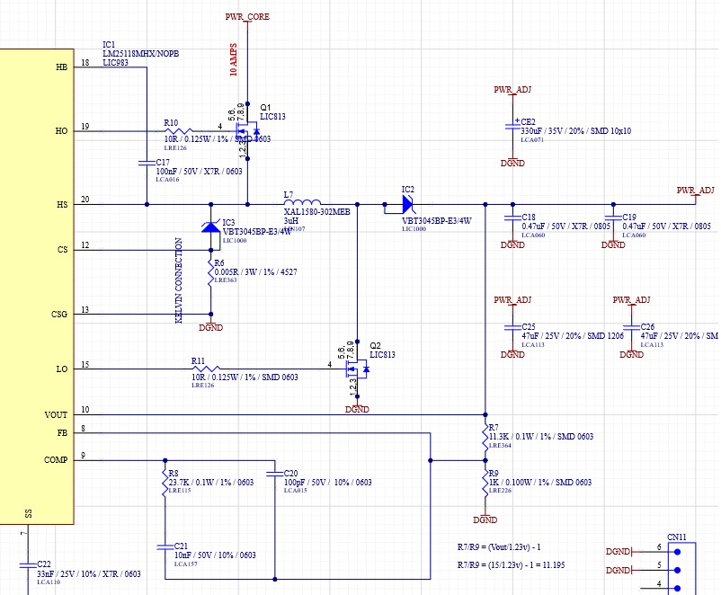
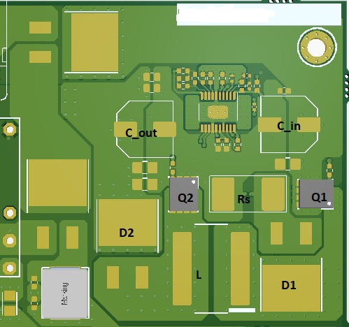
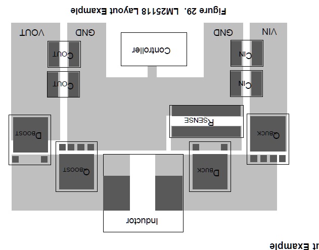
We have a layout based largely on the application note in the datasheet (snvs726f.pdf). The board is 4 layers, 2 Oz copper and is of sound construction.

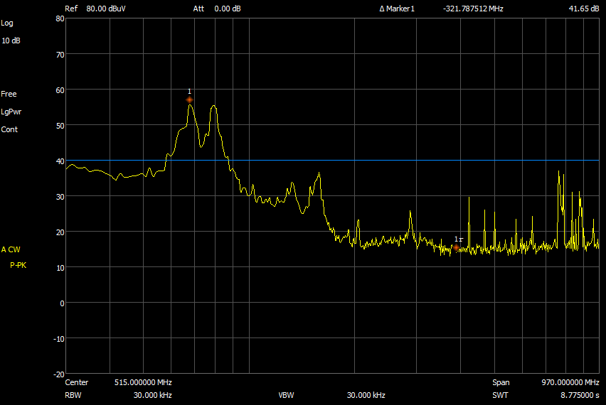
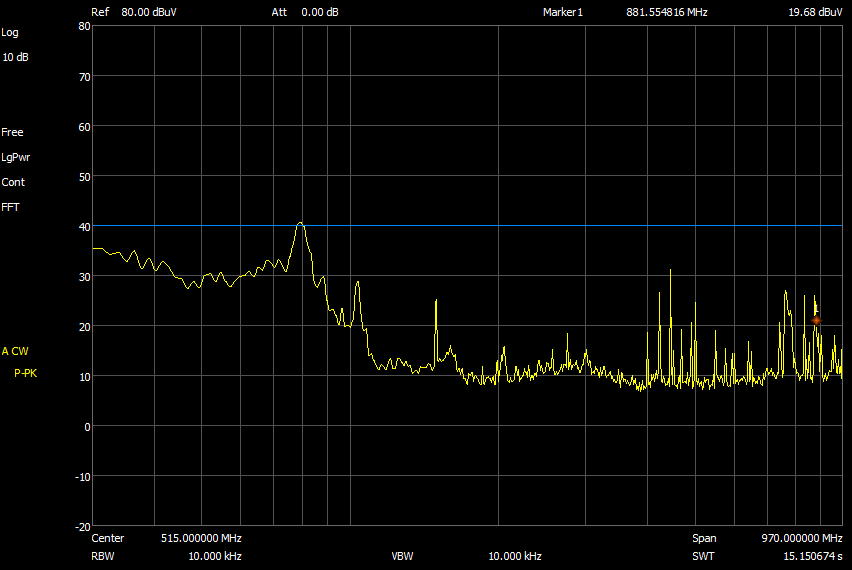
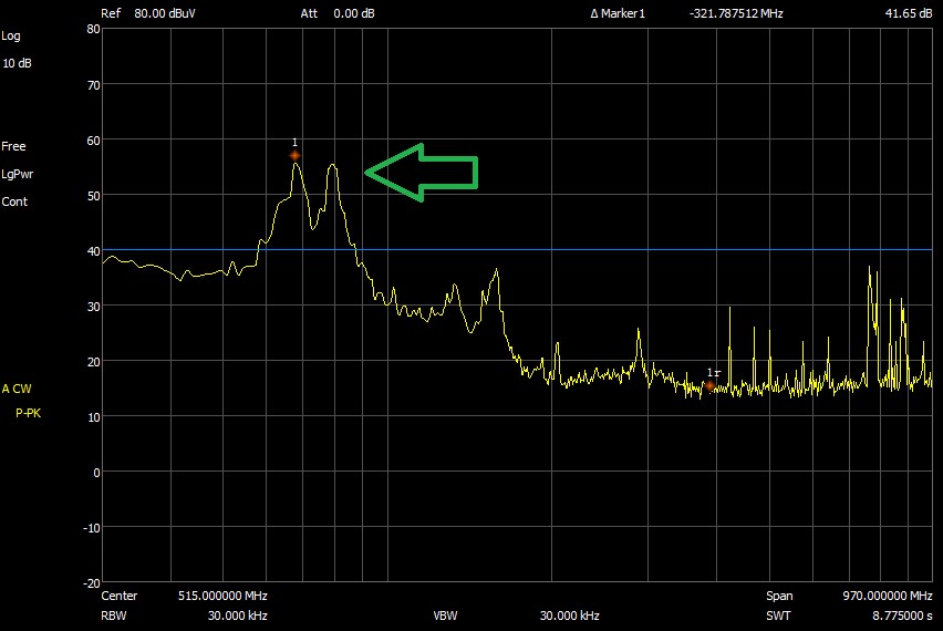
We note that during radiated emissions testing we have some large peaks at about 80 Mhz.

We have tried to build low pass LC filters on the output as well as add ferrites, and none of this reduces the noise by the 10 dB we require. Note that we have placed the filter past D2 (basically at the output of our device).

We have also tried slew rate control on our MOSFETS which have no effect.

I'm seeking TI's expert advice here as where we can look next. Are there other things we can do in-circuit to reduce the noise ending up in the output of our device?. Would the change to a shielded inductor likely help our cause? Anything else anyone can think of?

Thanks in advance.

  • Hello stomp,

    EMI issues are not easy to solve in general, so please expect recommendations that will not change the behavior.

    You mentioned that you tried to add LC filters and ferrite beads on the output. Did these components reduce the noise somewhat? Did you try to combine these if there was a reduction by one method?

    In the datasheet of the diodes I cannot find the information about the recovery time. Please try to get another diode in the same package with a fast recovery time.

    Please try to add high frequency ceramic capacitors very short from the high-side FETs to GND. Be aware that the capacitor has a frequency range of up to 100MHz.

    Check if you can reduce the length of connecting cables on VIN and VOUT. Often the connecting cables are antennas.

  • Hi Brigitte,

    The datasheet makes mention of a snubber requirement. As you mentioned, we figured that maybe our choice of diode had something to do with it and / or ringing in the edges of the switching at the inductor.

    To try and correct the problem, we placed a 680pF + 2.2R snubber from each side of the inductor to DGND. 

    We feel this approach is sufficient, however we are only using a home-made TEM cell for our EMC testing and will need to head back the lab for official results.

    For comparison:

    Before Snubbers:

    After Snubbers:

    Given the clear reduction in emissions using this approach I'll mark this as solved. Maybe TI could consider revising the snubber section in the datasheet and / or on the EVM to make it a bit clearer to designers of the challenges with using this part.

    Thanks

    Stomp!

  • Hello stomp,

    What about the EMI test result  now? can it pass in all the frequency range.  After adding RC snubber, high frequency range can be better, but sometimes, the low frequency range will getting worse.

  • Hi Helen,

    Yes we passed easily now.

    The key is the snubber and also we changed the slew rate control resistors on the gates of the MOSFETS.

    In general the gate resistors had the biggest effect in eliminating the ~80 MHZ noise.

    Thanks.

  • Good news!

    So in a summary, adding RC snubber is good for suppress the very high frequency noise while slowing down the switching speed is good for suppress the around 80MHz noise on your board, is it correct ?

  • Hi,

    I should have been a bit more clear about the testing and the results, after all if I had found the solution to my problem here I would have saved a few days work.

    We designed our hardware with a gate resistor in place on both the FETS, this is just our normal practice. We skipped over the snubber section in the datasheet as I've always felt snubbers are to patch problems that can be eliminated elsewhere in the design.

    At the lab, during an official conducted emissions test to CISRP-11 we had a peak of +10 dBm over the 40 dBm limit at about 80 MHz at 3 meters.

    We did a study of the gates of the FETs using a scope with appropriate spring clip probe right at the FET. We noticed that in the edge of the gate switching there was some ringing, the frequency of the ringing was about 80 MHz. We increase our gate resistor to about 22 R, which reduced the ringing, and we considered that this change did not have a thermal impact on our design.

    Changing the gate resistor reduced the peaks at about 80 MHz by about 10-15 dBuV in our TEM cell, this was a massive change.

    We still had broadband noise from about 30 MHz up to about 500 MHz and by adding the snubbers (680 pF + 2.2R) between each side of the inductor and ground. This reduced the overall broadband noise by about 5 dBuV in our TEM cell.

    Thanks

  • Hi stomp,

    Thanks for the update. Yes, drive speed will effect the around 80M EMI, this is in accordance with our test result too. For the snubber, it can help higher frequency EMI, but sometimes it will effect the low frequency EMI, glad to know the snubber has no side effect in your application.

    Good Luck! :)