This thread has been locked.

If you have a related question, please click the "Ask a related question" button in the top right corner. The newly created question will be automatically linked to this question.

LM3489: Heating issue in LM3489

Part Number: LM3489

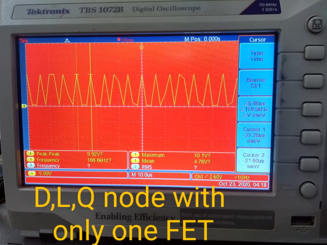
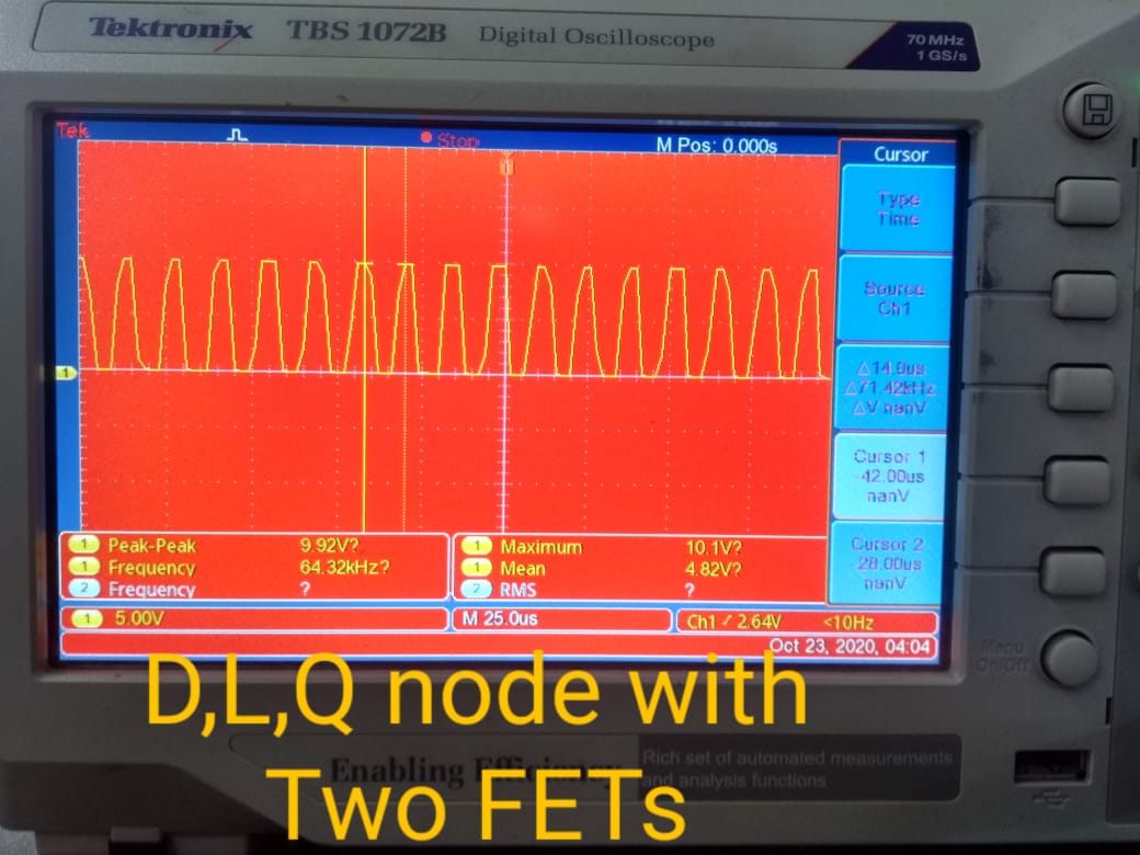
LM3489 is heating for lower switching frequencies. I have used it in 3 circuits.

12V to 12V- No heating

Circuit is designed for 5A, tested upto 2A load.

12V to 5V- Heating issue

Circuit is designed for 5A, buck starts heating for small currents as low as 50mA

12V to 3.3V - Heating issue.

Circuit is designed for 5A, buck starts heating for small currents as low as 50mA

Please find the below schematic for 5V conversion, the circuit is similar for the other 2 voltages as well.. Please let me know, why there is heating issue in the buck controller

  • Hello

    Can we have more clarification on the first design---12V to 12V ???

    Is the heating from the MOSFETs or the controller ??

    Also, please send your PCB layout layer views

    I will assign this to our controller team.

    Thanks

  • To TI.rar

    Dear Frank,

    I have attached the schematics of all the 3 buck conversions with layout. Is it something to do with the FB pin voltage or the switching frequency?

    As the FB pin voltage in the 12V to 12V conversion is 1.18V and in the other two buck conversions, it is 1.4 and 1.42. 

    In the schematics the values have been calculated for the feedback resistors for the buck conversions during design. But there seems to be some variations when observed practically.

    Or I have to reduce the switching frequency, using the formula given in the datasheet?

    Please check and revert back. 

  • Krishna,

    The feedback reference is 1.239V typically. This FB voltage or lower keeps the FET turn - ON.

    For your 12VIN to 12VOUT the converter is at 100% duty cycle, so I expect the output voltage to drop based on the FET RDSON and inductor DCR.

    Since at 100% duty cycle the 12V output has some resistive drop we expect the FB voltage to be less than the reference so 1.18V is OK.

    1.4V and 1.42V is large though. How did you measure this? Can you try probing FB node with an oscilloscope?

    See app note regarding PCB layout tips for thermals https://www.ti.com/lit/an/snva183b/snva183b.pdf

    Do you have top layer GND copper pour? If not I suggest drawing a GND polygon underneath the IC to help with heat spreading.

    Thicker traces and more GND thermal vias will also help move heat out of the IC.

    Hope this helps,

    -Orlando

  • Hi Orlando,

    I shall measure in the scope and get back. Any corrective resistive values from your end for the FB pin ?

    Did you go through the schematics attatched?

    Is there anything else which needs corrections?

    What else can be the reason for heating?

    Is it due to the high switching frequency of the IC?

    Pls review and let me know your comments.

  • Krishna,

    As shown in figure 19 of the LM3489 datasheet FB node voltage is regulated to lower value of Vref or 1.239V, and will have at least 10mVpp of ripple.

    The output voltage equation based on a resistor divider is then VOUT = VREF * (1 + Rfbt/Rfbb).

    For the 5V design I get VOUT = 1.239 V * (1 + 62k/20k) = 5.08V.  I also get 3.295V and ~12.02V so those resistors are correct.

    Also on that same page the switching frequency in equation 4 depends on alot of variables, and is non trivial to calculate.

    If you can scope shot the Switching node (node of FET, diode, and inductor) that would be great for confirming stable operation.

    Actually I think the dual-FETs are contributing to this issue. The FETs connected in parallel will halve the RDSON but it will double the QG gate charge. 

    Double the gate charge will negatively affect FET rise and fall times, increase switching losses, and negatively contribute to thermals.

    This would not appear in the 12V as it is 100% duty cycle and not switching.

    Please check the PGATE rise and fall time and also only with a single MOSFET.

    -Orlando

  •                   

    Dear Orlando,

    PFA the scope shot of the switching nodes as specified by you. I can say there is only a slight reduction in the heating when only one MOSFET is used, nothing has changed drastically.

    The FETS I have used is FDS4435BZ. 

    Also, now I have changed the feedback resistors to 60.7k exactly instead of 62k and also, the inductor used is a 22uH. But practically the heating difference is not much, even for a load of 50mA there is significant heating upto 34C, the ambient temperature here is around 20 to 22C

  • Krishna,

    What is the output current of these scope shots?

    The switch node rise and fall time look very long, like several microseconds?

    SW node should be a square wave, please check if the PGATE output is square.

    I do not think 34C is too hot but it depends on the load. 

    You can try reducing the switching frequency by increasing the inductor and there should be improvement.

    Your powerstage layout could be improved, switch node routing is not optimal and I think this is contributing to slow slew rate.

    See video on buck powerstage. 

    https://training.ti.com/power-tips-layout-buck-power-stage

  • Output current is around 50 to 70mA for the scope shots

    Yes the switch node rise and fall time is around 14us

    Ok will check it.

    I am attaching a temperature testing data starting from minimum load for around 1hr.

    Yes yesterday already I have changed the inductor value to 22uH from the original design with 15uH. Also yesterdays scope shots are captured with the 22uH inductor value.

    Yeah I shall work on the powerstage layout.

    PMU_5V section test_2020-10-22.xlsx

  • Krishna,

    14us is very long, increased SW node rise and fall times will affect the switching losses in the PFET and FET will be hotter. Better SW layout should help with faster rise time. 

    Your temperatures at high current are expected, at low current it is a bit hot. I'm not sure why the device is not in discontinuous mode like figure 16 of LM3489 datasheet), are you able to scope the inductor current with a loop (on VOUT side)?