This thread has been locked.

If you have a related question, please click the "Ask a related question" button in the top right corner. The newly created question will be automatically linked to this question.

UCC28180: UCC28180, TIDA00652

Part Number: UCC28180
Other Parts Discussed in Thread: USB2ANY, DRV10983,

Hello

1. Can I test the TIDA00652 design , with a DC electronic Load?  I have been testing my design based on the reference circuit along with DRV10983 + USB2any to set constant load of a bldc motor, I have some issue with few board which I have to test with constant load.

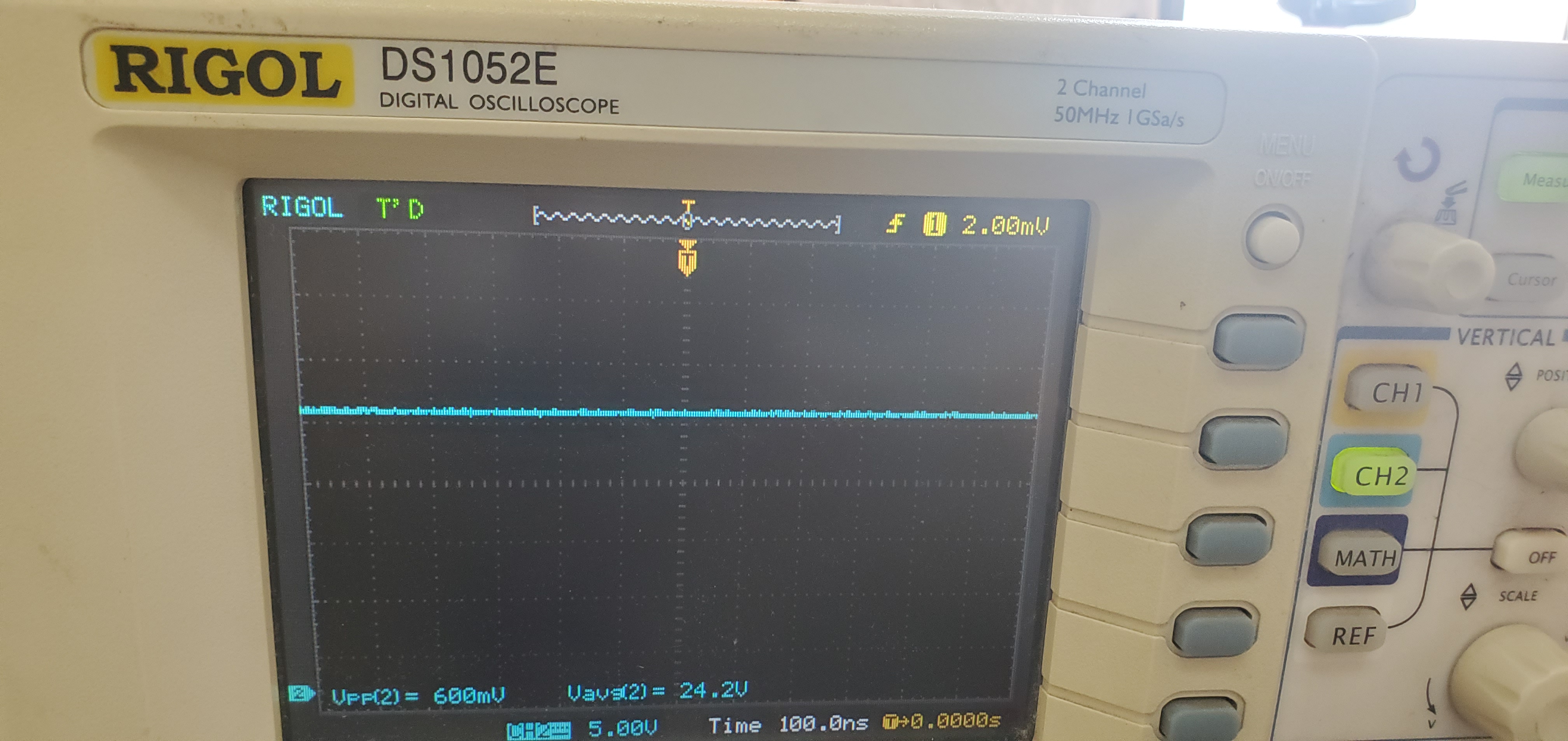
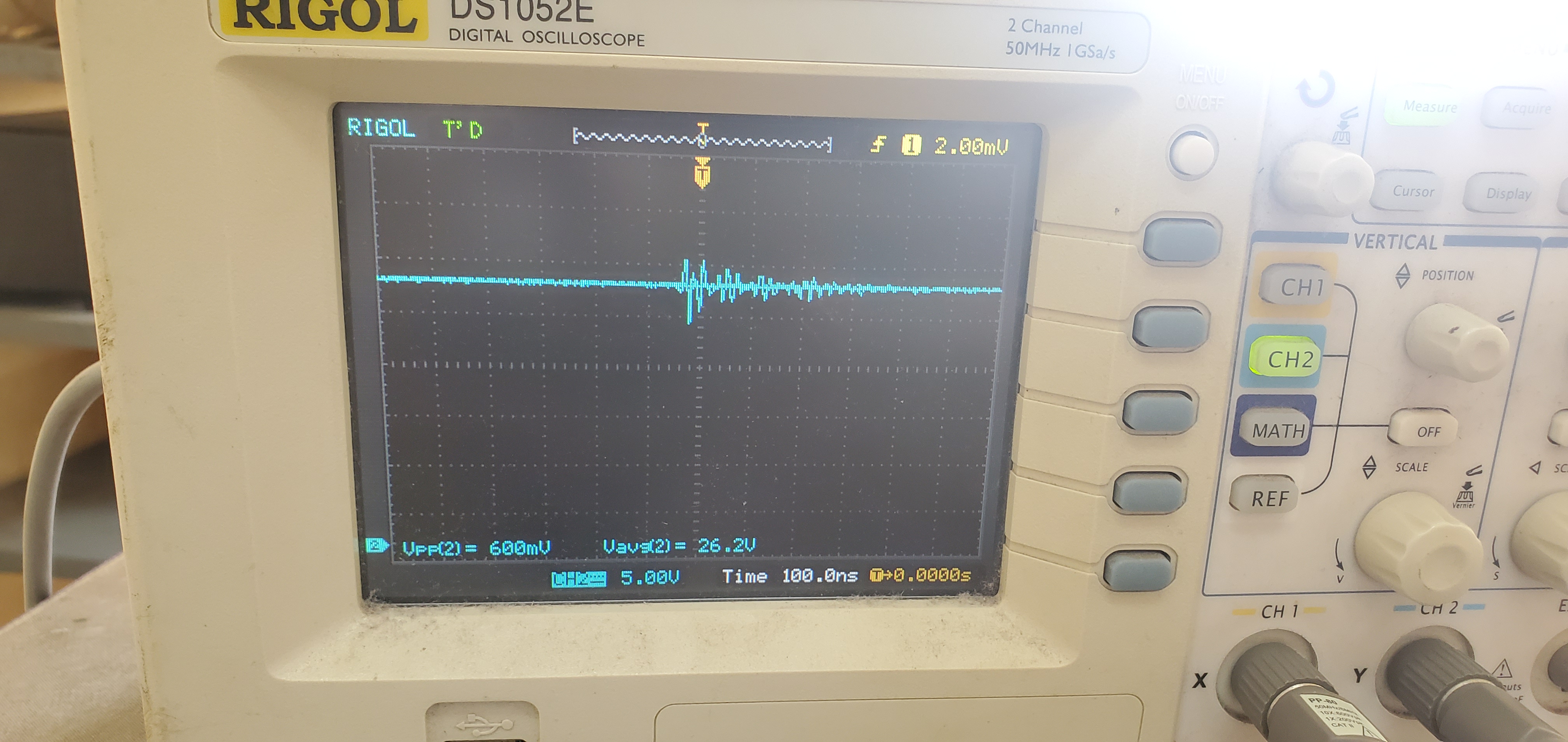
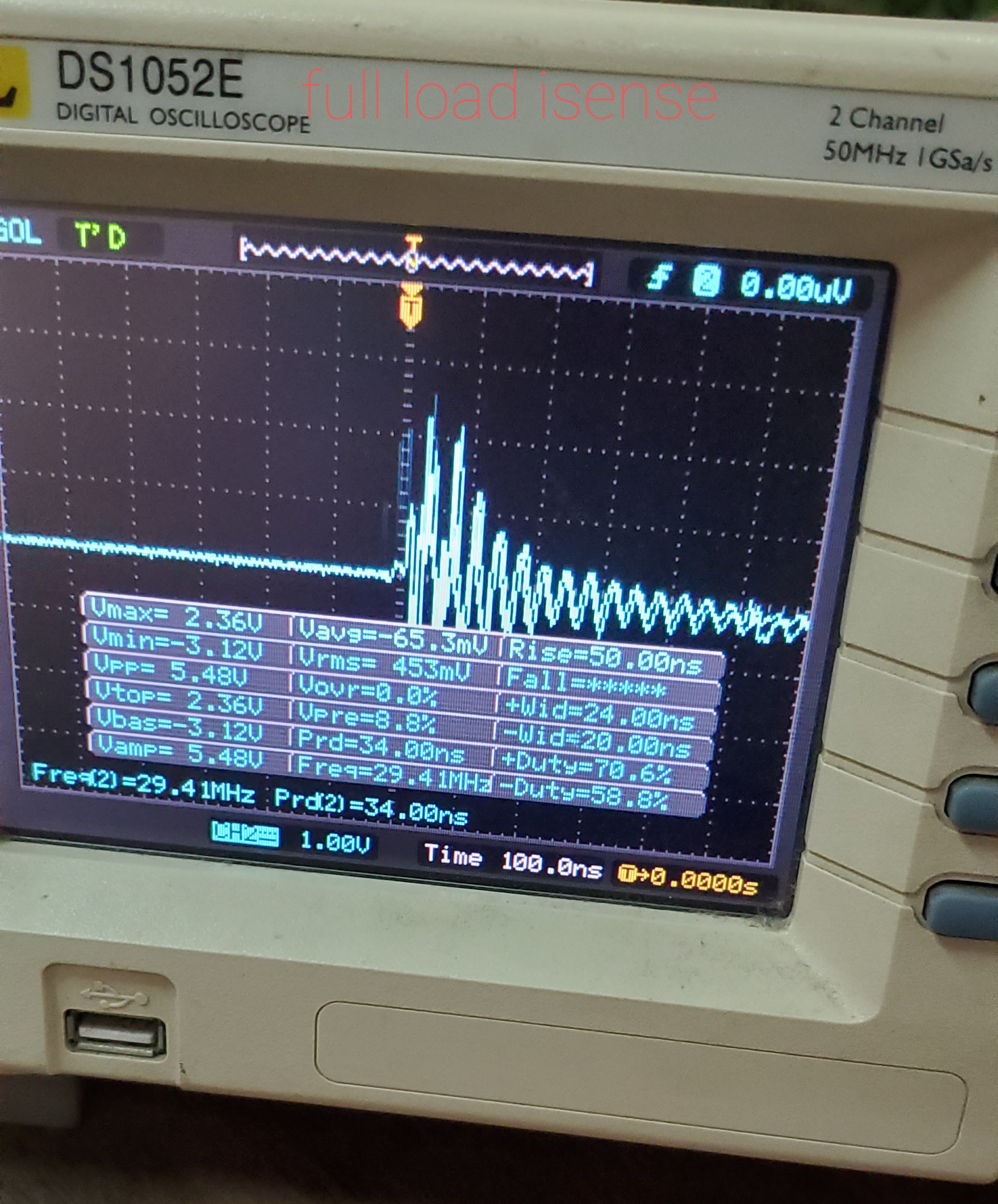
2. TIDA00652 , has been working fine , but I am facing some issues some  boards, they can't seam to follow the actual current control, That is  when I try to run the motor load of around 12W at 24V ( current draw should be 0.5 to 0.6 amp), the input current draw crosses 0.250Amp, and the power supply goes in protection, all the components on the working boards and the boards that have this issue are same. The output of the power supply stays between 23.9 to 24.6 volts , even the DRV reads similar voltage, but the voltage at TP2 increase from 4.9 at standby mode to anywhere between 15 to 30 volts.

The test rig used is same for all the boards, including the DRV board.

  • Hi Dinar,

    An expert will get back to you soon !

  • still awaiting to hear from an expert regarding the issue.

  • Hi Dinar,

    you can use TIDA00652 with electrical DC load or resistor load. And please pay attention that the reference design engineer suggest not to power on the the board with heavy load, so I suggest power on at no load condition, and step by step increase the power.

    For the issue you met, I would suggest you can use a DC source to power on the motor driving. The aim is to identifiy whether the issue is in UCC28180 stage or for the motor stage.

    do you build  boards by yourself following TIDA00652? Or the issue is happened at TIDA00652?

  • Hi David

    Thank you for your reply.The dummy load will be to used  test  the circuit at fixed loads, from no load condition to max load of 30watts ( 1.25Amp output), and also  overload conditions, I have want understand the working of the circuit .

    Is there any specific reason why the design guide  for testing suggest a fluck multi meter for current measurement  on the output stage between the power supply and resistor bank? 

    As for the un-controlled current on some boards, I have figured the reason the PCB itself is causing the issue, the substrate used by the manufacturer for some PCB is wrong it seams, I am still trying to find out if the boards have leakage at higher loads.

    I have designed my own double sided PCB , the design is stable with the new PCBs .

    Thanks and Regards

  • Hi Dinar,

    thanks for your information.

    There is no specific reason for the current meaure. Using Fluck multi meter is a simple way to do this, you can also use a high precise resistor in series into the line and directly test the voltage on the resistor and calculate the current.

    thanks.

  • Hi David

    Thank you for the reply. My design for resistive load will start from 240 Ohms for 0.1A At 24 vdc (2.4W) and drop to 19.2 ohms for 1.25A at 24vdc  (30W) in steps.   these resistive load should  work for the TIDA00652 reference design? please correct me if I am wrong.

    Thanks and Regards

  • Hi Dinar,

    yes, you are correct.

  • Thank you for your reply, will update once I build and test the dummy load.

  • Hi David

    I have tried to check the TIDA00652 without load on power up, while checking for voltage between TP3 and TP2 , there is mild ticking sound and also the output voltage jumps from 24.1Vdc to 28 and more, even after removing prob from TP3 and TP2 , unloaded voltage remains high in unloaded state, but with a small load ( in my case DRV without any motor) the voltage jumps to 26 and remains there till the prob at TP2 is connected.

     All the components are as per the BOM.

    As per my knowledge usually clicking noise is due to either switching frequency being very high( above designed value for the inducter) , overload condition, or ground noise , in my case the switching frequency is same on both boards as the resistor values is 21.5K. inductor is 34uH on both , MOSFETs are same make and specification. PCB are batch and high quality (nano gold plated).

    I have tried all solution as per my knowledge about the design , but few boards have this issues.

    I am adding oscilloscope waves for 2 boards, one works as per design, PCB design is same components are from same reel.

    The above photos shows the output of the power buck converter that has DRV connected as load (no motor is connected) , so the standby voltage , the 1st photos is only the output, the 2nd photo is shows the output will multimeter connected to TP3 and TP2. the output jumps to 27 and settles to 26.2V and clicking sound starts, it corresponds to the oscillations of the wave.

     Below photos show the output at same testing setup of the board the board that works as designed, again same PCB design, components from the same reels, but there is no clicking sounds.

    I have confirmed that the output capacitors are as samilar capacity on boath and the ESR for all ( I am using 2 X2200uf /35v cap)

  • Hi Dinar,

    sorry for delay response。

    are you able to find the difference between the "bad" and the "good"boards?

    Please replace the device step by step and try to find the difference.

  • hello David

    Thank you for your reply.

    I did replace all the components from a working board to a non working board, yet there is are some issues.

    There was a issue with capacitor on Vcomp (pin 5) , C26 was wrong. so it had issue starting and holding PWM. now the clicking sound is cleared, but the boards which had this issue are having trouble going to full load. the PWM jumps from a controlled width to a large PWM width at around 17watt( input current is at around 0.050A at 230volt) , the boards that work where working are going to full load and can hold the input current upto 0.150A at 230 volt.

    I could no find calculation for capacitor values of the design , have I missed and application note ?

    I can't seam to keep the boards ( all boards) loaded and measure voltage between TP3 and TP2 , as soon as meter or oscilloscope probe is connected , the board switches off and clicking sound appears.

    I will uploads photos of waves for both working and none working boards in sometime.

    Thank you

  • Hi David

    I am attaching waveform of a working board and none working board, there is alot of noise on the Isense signal when the MOSFET gate is triggered hence the UCC28180 switching off and turns on .

    above are  full load isense and Gate drive signal at pin1 of UCC28180

    below photos are at standby ,19watt. all photos are of working board.

  • board which have trouble holding required current 1st is since at standby , 2nd is trigger at the pin of ucc28180, there is large spike which is positive . Also such boards have voltage on TP3 as well, when the power supply is loaded.

  • Hi Dinar,

    Since there are not too much devices on those two boards, I know you have alrready replace all the device except the Pcb. 

    Is it possible to replace the device on the "bad"board on the "good"pcb?

    actually I still can not identify why there are big difference between two boards with the same parameters.

  • one moare suggestion is that can you please increase the turn on resistor to limit the ocilation on the driving? From your waveform, there are big oscillation on Gate driver signal.

  • HI David

    replacing the components, was done replaced from the working to the none working board, but same result. components are not a issue here.

    the non working boards seam to get a high isense voltage when the Mosfet is triggered, it is suppose to be in negative and uV to mV, and the spike is 1 to 4 volt when the mosfet triggers but the board that have issue the voltage fluctuates from negative to positive and the spike is upto 6 to 14 volts, I believe this is why the current (PWM) has issue stabilizing as per demand.

    I cut the gate drive track and used a wire to confirm , and the boards seam to work after failing to to go to full for 2 to 3 time, it is repetitive every time the power supply is turned on.

    Regards

  • David Huang33 said:

    one moare suggestion is that can you please increase the turn on resistor to limit the ocilation on the driving? From your waveform, there are big oscillation on Gate driver signal.

    will increase the resistance on the gate drive and check.

    Thank you

  • Hi David

    your suggestion for resistance increase has solved the noise issue and the boards are working , have connected load and testing the boards for any other variations.

    Thank you very much for your time, will update about results soon.