This thread has been locked.

If you have a related question, please click the "Ask a related question" button in the top right corner. The newly created question will be automatically linked to this question.

TLV767: Typical Application Circuit in the datasheet

Part Number: TLV767

Hi there,

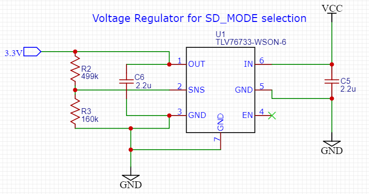
I was needing a voltage regulator to achieve 3.3V from a 5V input and come across this product and its conveniently detailed Typical Application Circuit (Section 8.2 of the datasheet).  This provides nominal resistor values to achieve my 3.3V output.  This was great.  I've just received my PCB's and built the circuit and am measuring just over 4V from the TLV767.  Why is this?  Is there an error in the design provided in section 8.2?  It seems correct...

Any assistance would be greatly appreciated.

Kind regards.

  • Hi Mark,

    Can you provide a schematic of your circuit?  Also please confirm that there are no voltage rails back feeding the LDO which can raise the output above 3.3V.

    Thanks,

    - Stephen

  • This is it.  Ignore Pin7, it doesn't exist on the circuit, it was just in the TLV model I found in EasyEDA.  As per the Pin Functions table in Section 5, the EN pin has been left floating to enable the device.

    Thank you!

  • The schematic looks correct to me. If you are measuring just above 4V on the output, that would suggest Vref is about 1V which is incorrect.  What might be happening is leakage on the board pulling the SNS pin low, which looks like a parallel resistor to the 160 k-ohm resistor.  A leakage path which forms about 550 k-ohms of resistance in parallel with the 160 k-ohm resistor would be enough.  Customers contact us about once every other month with an issue like this which ends up being a leakage problem.

    If a thorough inspection and cleaning of the PCB does not correct the issue, we'll need some oscilloscope waveforms of Vin and Vout to continue the troubleshooting.

    Thanks,

    - Stephen

  • OK.  I'll give the board a thorough clean and try again.  I'm surprised though, they are brand new and apparently clean boards.  Looking at the first layout example in section 10.2 of the datasheet (which I used in designing my PCB layout) where would this leakage need to occur to cause this problem?  I'll focus my inspection attention there...

    Also, side question, I thought any leakage current would cause the resistance to go down, not up?!

    Thank you!

    Kind regards,

    Mark

  • Even brand new boards can have this issue.  We occasionally see this with new boards from large customers.  Excessive flux can be cleaned through a DI bath or by using a flux cleaner.  If we find that cleaning the boards fixes the issue, you may want to request a cleaning step in the board assembly if that is not already being done by the assembly house.

    If the leakage path brings down the resistance from SNS to GND, then Vout will go up.  As an example:

    If R2 = 2k and R3 = 1k, then Vout would be approximately 0.8*(2k+1k)/1k = 2.4V.  But if leakage across R3 forms a parallel resistance, it will go down.  Lets assume R3 becomes 500 ohms.  Then Vout = 0.8*(2k + 500)/500 = 4V.

    You will want to focus on the SNS pin and the GND pin as well as the thermal pad (which is tied to GND).

    Thanks,

    - Stephen

  • Thank you for the detailed explanation.  That's just the information I needed to be able to explore this further.  

    Kind regards,

    Mark

  • Sorry.  I forgot to add.  What can I do to my current board to get the output Voltage down to 3.3V again?  Can I add or swap resistors?  Or will the leakage still be a problem?

    Thanks!

  • If the issue is due to leakage then once you clean the board you will find that the issue goes away. 

    If leakage is not the issue, it could be that the resistors were installed incorrectly or the component was somehow damaged.  In this case I would gently remove the resistors and test them with a DMM to confirm they are correct.  If that does not work then all that is left is to remove the LDO and replace it with a known good unit.  Each time you remove and replace a component you will want to be sure that the board is clean. 

    If the issue goes away but only after the IC was swapped, you can do what we call an "A-B-A" swap to see if the issue follows the LDO.  You may wish to perform the A-B-A swap on an EVM to avoid any issues with your actual hardware.  An A-B-A swap is removing the IC associated with the problem, placing a known good or brand new IC on the board to see if the issue goes away, then removing the known good IC and placing the old IC back onto the board to confirm the issue comes back.  This removes a number of failure modes associated with the board and circuitry and locates the root cause with the original component to aid in troubleshooting.

    Thanks,

    - Stephen